
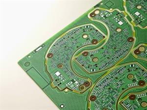
HDI technology is rapidly expanding in the PCB world. This technology allows significantly denser and smaller board construction and packaging allowing for substantially more components per square inch. Basically, it’s more technology-functionality in less space. HDI has proven invaluable and critical in the production of electronic equipment with smaller and tighter space. Cell phones, laptops, and high speed performance and computing would not be possible without HDI as we know it today.
Examples of HDI technology include fine lines and spaces, sequential lamination, back-drilling, non-conductive and conductive via fill, blind vias, buried vias, and microvias. These are specifically PCB technologies that are allowing tight and miniaturized packaging. They also allow higher levels of performance like controlled impedance and satellite technologies. Designing and manufacturing HDI PCB’s comes with an increased cost, but one that must be embraced and mastered to meet the ever demanding requirements of the Electronic Industry.