
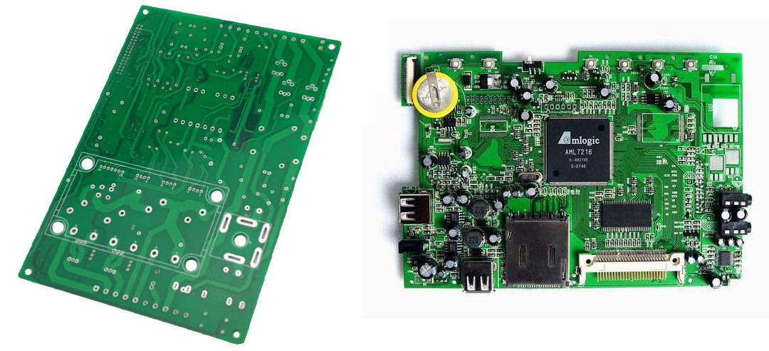
A PCB (Printed Circuit Board) is a board that electrically connects electronic components using conductive traces, pads, and other features etched from copper foil laminated onto a non-conductive substrate. PCB’s can be single sided (one copper layer), double sided (two copper layers), or multi-layer (outer and inner layers). Conductors on different layers are connected with vias (plated-thru. holes). Multi-layer PCB’s allow for much higher component density and design complexity.
A PCBA (Printed Circuit Board Assembly) is the board after all the components and parts have been soldered and installed on the PCB and now can accomplish the electronic function it was designed for.