Engineers building these products run into the same wall: fine-pitch components that standard pick-and-place equipment can't handle reliably, signal integrity problems that only show up at speed, thermal hot spots from packed-in components, and design flaws that surface only after fabrication — when a respin costs weeks, not days.
This article breaks down the core techniques that make complex PCB assembly possible, the testing methods that catch defects before they reach the field, and what to look for in a manufacturing partner capable of executing builds like these without the usual delays.
Key Takeaways
- Microvias, fine-pitch placement, and controlled impedance routing enable reliable high-density PCB assembly.
- AOI, X-ray, and flying probe testing catch defects standard visual inspection misses.
- Separating PCB fabrication from PCBA planning keeps build timelines accurate and realistic.
- Single-source fab-and-assembly partners cut cycle time and end cross-vendor blame.
What Is Advanced PCB Assembly?
Advanced PCB assembly covers builds that go past standard SMT and through-hole work: higher layer counts, tighter tolerances, fine-pitch or leadless components, and specialized processes that most contract manufacturers don't offer as a matter of course. You'll find it most often in aerospace, medical, automotive, and defense programs, where a failure can be dangerous, not just expensive.
Standard assembly, by contrast, typically means 2-4 layer boards, larger components with generous spacing, and looser tolerances that leave room for error. Complex builds don't have that room.
That gap is why the line between bare board and finished assembly matters so much on complex work.
PCB vs. PCBA: Why the Distinction Matters
A PCB is the bare, unpopulated board that comes out of fabrication. A PCBA is that same board after every component has been soldered on. They're two separate manufacturing stages, and on complex designs, keeping both under one roof matters more than it might seem.
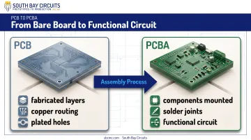
When fabrication and assembly happen at different companies, every stackup question, impedance tolerance, or via-in-pad decision has to be relayed between teams that never talk directly.
South Bay Circuits handles fabrication and assembly at its 60,000-square-foot Chandler, Arizona facility, with PCB fabrication spanning double-sided boards up to 22 layers. That in-house structure means design questions get answered by the people actually building the board.
"Complex" generally means one or more of the following:
- High pin-count BGAs or fine-pitch QFNs
- HDI construction with blind or buried vias
- Rigid-flex assemblies
- High-speed digital or RF signal requirements
Each of these needs engineering input starting at the design stage — not after the Gerbers are finalized.
Core Advanced PCB Assembly Techniques for Complex Designs
Executing these techniques takes specialized equipment and engineers who've done this before. On mission-critical electronics, a deviation of a few thousandths of an inch can mean the difference between a working board and a field failure.
Microvias & HDI Technology
Laser-drilled microvias let designers pack far more interconnections into the same board footprint, a requirement for miniaturized, high-layer-count boards. The global HDI PCB market is forecast to grow at a projected 8.5% CAGR from 2026 through 2033, reflecting strong demand for this density.
Getting microvias right means controlling drilling, plating, and insulation with precision. South Bay Circuits supports microvia diameters down to 0.004 inches, verified through cross-sectional analysis and test coupon inspection on every panel.
Fine-Pitch & Leadless Component Placement
Sub-0.4mm pitch components (BGA, QFN, and micro-BGA packages) leave almost no margin for placement error. This level of work requires:
- High-precision pick-and-place equipment with vision alignment
- Solder paste inspection (SPI) to catch paste volume issues before reflow
- Automated optical inspection (AOI) to flag misalignment or bridging early
South Bay Circuits places fine-pitch components down to 0.4mm with engineering review, and supports standard 0201 package placement using its in-house Fuji chipshooters and AOI systems.
Controlled Impedance Routing for Signal Integrity
High-speed and RF designs live or die on trace width, spacing, and dielectric selection. Get the stackup wrong and you're chasing EMI problems or signal degradation after the board is already built.
This is why design and fabrication engineers need to be talking about stackup before production starts, not after a prototype fails testing. South Bay Circuits validates impedance through Polar TDR testing and supports impedance-control targets as tight as ±5%, across structures including edge-coupled stripline and coplanar waveguide.
Advanced Soldering Methods for Mixed-Technology Boards
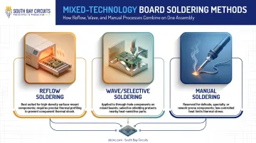
Boards that combine SMT and through-hole components need more than one soldering approach. Reflow handles surface-mount work, wave or selective soldering covers through-hole parts, and sensitive or oddly placed components sometimes need a trained hand instead of a machine.
Solder profiles have to match each component's thermal sensitivity — push too hard and you get voiding or heat damage on a densely packed board. South Bay Circuits runs both convection reflow and dual-pot wave soldering in-house, with manual soldering available for specialty components that don't tolerate automated processes well.
Conformal Coating & Underfill for Reliability
Fine-pitch components exposed to moisture, vibration, or thermal cycling won't survive long without protection. Conformal coatings and underfill guard against exactly that, which is why they're standard on aerospace and automotive builds operating in harsh conditions.
This becomes non-negotiable when a board needs to meet IPC Class 3 or MIL-SPEC workmanship standards. South Bay Circuits offers silicone, acrylic, and urethane conformal coatings as part of its assembly services, applied to protect against moisture and chemical exposure in the field.
Rigid-Flex & Multi-Board Stackup Design
Rigid-flex construction eliminates cabling and connectors by folding what used to be separate boards into one flexible assembly. It saves space and removes failure points. Connectors are notorious for vibration-related issues.
Getting there requires careful planning around:
- Bend radius limits for the flex sections
- Layer transition zones between rigid and flex areas
- Thermal management across the combined stackup
South Bay Circuits supports flex and rigid-flex materials, including polyimide substrates, within its standard PCB manufacturing capabilities.
EMI/EMC Shielding Strategies
Densely packed circuits interfere with each other, and regulators don't give you a pass for it. Board-level shielding (cans, conductive coatings, and grounding strategies) keeps interference contained and helps designs meet EMC requirements before they ever reach a test lab. South Bay Circuits includes EMI shield coating among its assembly-level services for builds that need this added layer of protection.
Common Challenges in Complex PCB Assembly
Even with the right techniques, complex builds run into predictable friction points.
Component miniaturization and obsolescence. Fine-pitch and leadless parts are harder to source, and on long-lifecycle aerospace or medical programs, components can go end-of-life mid-production. VMI, JIT, and Kanban inventory programs help manage this risk by keeping replenishment aligned to actual consumption, reducing shortage exposure on hard-to-source parts.
Thermal density. More components in less space means heat has fewer places to go. Thermal vias, heavier copper weights, and via-in-pad techniques all help move heat away from hot spots. Via-in-pad places a via directly under an SMT pad, then fills and plates over it so you save board area without losing thermal or electrical performance.
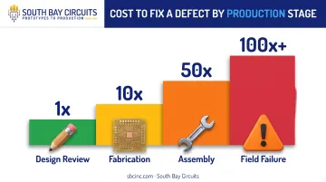
Skipping design-for-assembly review. This is the costliest mistake on complex boards. Once a board is fabricated, the physical layout is locked; problems like connector-shell interference or inadequate test access can only be worked around, not fixed cheaply.
As PCD&F's engineering analysis notes, rework or PCBA revisions at assembly cost far more than catching the same issue in design. A DFM/DFA review before layout is finalized is the lowest-cost way to avoid those problems.
Quality, Testing & Inspection Methods for Complex Assemblies
Complex assemblies hide defects that a visual check simply can't catch. A layered testing approach is the only reliable way to verify a board actually works as designed.
Automated optical inspection (AOI) catches missing components, solder bridging, tombstoning, and lifted leads — but it can't see under a BGA or QFN.
X-ray inspection fills that gap. It verifies hidden solder joints, voiding, and internal via connections on multilayer and HDI boards. South Bay Circuits uses X-ray equipment specifically for BGA and IC inspection, checking for shorts and poor solder connections that AOI would miss entirely.
Beyond visual and X-ray checks:
- Flying probe testing validates electrical connectivity without a dedicated fixture, making it well suited to NPI and frequently revised designs
- ICT (in-circuit testing) catches component-level opens, shorts, and wrong values on more stable designs
- Functional testing confirms the board performs its intended job, not just that it's electrically sound
Those methods only hold up when judged against recognized acceptance criteria. IPC-A-610 defines workmanship acceptance standards, while J-STD-001 governs the soldering process itself. South Bay Circuits builds to IPC-A-610 Class II or Class III depending on program requirements, and supports IPC-6012 Class III for military-grade PCB products.
Choosing the Right PCB Assembly Partner for Complex Designs
Not every contract manufacturer that says they "do complex boards" actually has the equipment or experience to back it up. A few questions separate the ones who do from the ones who don't.
Ask for comparable examples. Request case studies or sample builds involving HDI, rigid-flex, or fine-pitch work similar to yours. If a partner can't point to relevant experience, keep looking.
Check certifications against your industry:
| Certification | Relevant Industry | Why It Matters |
|---|---|---|
| ISO 9001:2015 | All | Baseline quality management system |
| ISO 13485 compliance | Medical devices | FDA CGMP alignment under 21 CFR Part 820 |
| ITAR registration | Defense | Required for handling defense articles/technical data |
| CMMC Level 1 | Defense | Protects Federal Contract Information |
| IATF/TS 16949 | Automotive | PPAP and automotive quality requirements |
Evaluate in-house versus outsourced capability. A single-source manufacturer eliminates the shipping and queue time that piles up when fabrication and assembly happen at separate vendors, and it removes the finger-pointing when something goes wrong.
South Bay Circuits is ISO 9001:2015 certified, ITAR registered, and CMMC Level 1 compliant. The company runs fabrication and assembly under one roof in Chandler, Arizona, with 24-hour PCB fabrication and same-day assembly for time-critical builds. In one documented NPI comparison, a standard 23-day PCBA process was cut to 13 days (a 43% reduction) by removing coordination gaps between separate vendors.
Confirm NPI support. A strong partner reviews your Gerbers and BOM before committing to production, flagging design issues while they're still cheap to fix.
Review testing depth and turnaround commitments. AOI, X-ray, and flying probe capability should be in-house, not subcontracted. Subcontracted testing adds the exact delay you're trying to avoid on a complex build.
Frequently Asked Questions
What is an advanced assembly PCB?
Advanced PCB assembly uses high-density, fine-pitch, or specialized techniques (HDI, controlled impedance, rigid-flex) that go beyond standard SMT or through-hole work. These boards typically show up in aerospace, medical, defense, and automotive applications.
What is the difference between a PCB and a PCBA?
A PCB is the bare fabricated board with no components attached. A PCBA is that same board after full population and assembly: the two sequential stages of the manufacturing process.
What certifications matter most for advanced PCB assembly?
ISO 9001 provides a baseline quality system, while ISO 13485 (medical), AS 9100 (aerospace), and ITAR/CMMC (defense) address industry-specific compliance. Choosing a partner with the right certifications reduces audit risk and liability exposure.
How long does advanced PCB assembly typically take for complex designs?
Timelines vary with complexity and volume. Many manufacturers offer expedited prototype turnaround (sometimes same-day), with longer schedules for full NPI qualification and production runs on high-reliability builds.
What industries require advanced PCB assembly techniques?
Aerospace, defense, medical devices, automotive/EV, and industrial instrumentation lead the list. Each depends on reliability and miniaturization that standard assembly processes can't consistently deliver.
What is the difference between HDI and standard PCB assembly?
HDI uses microvias and higher interconnect density for compact, high-performance boards; standard designs use larger traces and vias. The difference is mainly in bare-board construction, but HDI's tighter tolerances also require more precise assembly.