Most designers who've debugged a misbehaving power rail know the symptoms: unexplained noise coupling into sensitive circuits, thermal hotspots that show up only under sustained load, and output voltage that sags the moment a load transient hits. These aren't component problems. They're layout problems.
This guide walks through regulator selection, layout best practices for grounding and component placement, thermal and EMI control techniques, and the mistakes that send boards back for a costly respin.
Key Takeaways
- Layout, not just component choice, determines noise, heat, and stability on power rails
- Choose switching regulators for efficiency, linear regulators for clean output
- Keep decoupling capacitors within a few millimeters of IC power pins
- Size trace widths and copper weight using IPC-2152, not guesswork
- Run thermal and power-integrity checks before, not after, fabrication
What Is a Power Supply PCB and Why Layout Matters
A power supply PCB is the section of the board (or a dedicated board) that converts incoming AC or DC power into the clean, stable voltages every other component depends on. It's a chain of conversion stages, each with its own layout requirements.
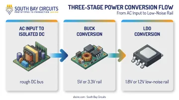
A typical power flow looks like this:
- AC input to isolated DC — a transformer, rectifier, and filter stage convert wall power to a rough DC bus
- Buck conversion — a switching regulator steps that bus down to an intermediate rail, often 5V or 3.3V
- LDO conversion — a linear regulator cleans that intermediate rail down to a low-noise 1.8V or 1.2V supply for sensitive ICs
Modern processors, ADCs, and FPGAs run on these low sub-2V rails, and they're unusually sensitive to ripple. Low-noise 1.8V analog rails are particularly vulnerable to noise in the 100 kHz to 1 MHz range — exactly where switching regulators generate their harmonics. That means layout quality on the final stage matters as much as which regulator IC you picked. Getting there starts with locking down the right specs early.
Before you place a single trace, nail down four parameters:
- Required voltage(s) for every rail on the board
- Maximum current each rail must supply, including transient peaks
- Acceptable voltage ripple for the most sensitive downstream component
- Permissible heat loss given your enclosure and airflow
Skipping this step is a common source of rework. A 2022 IEEE reliability review found the PCB itself carries a 26% failure chance within power converter systems, ranking it the second-highest failure contributor after semiconductors.
This figure comes from an IEEE lifetime-management review of power electronic systems and is converter-specific, not a blanket electronics statistic. Still, it makes a clear point: the board itself is often the weak link.
Choosing the Right Regulator: Linear vs. Switching
Regulator selection sets the ceiling for how clean and efficient your rail can be. Layout can't fix a fundamentally wrong topology choice.
Linear regulators pass current through a controlled resistance, dropping excess voltage as heat. They're simple, produce very low output noise, and need almost no external components. The tradeoff is efficiency — anytime the input-to-output voltage gap is large, most of your power turns into wasted heat.
Switching regulators use a MOSFET switching at high frequency (PWM) to convert power with far less loss. They stay efficient across a wide range of input-output ratios, but that switching action generates noise that couples into nearby traces and radiates as EMI.
Texas Instruments ran a direct comparison converting 24V down to 5V at 100 mA, and the numbers make the tradeoff concrete:
| Metric | Synchronous Buck | Linear (LDO) |
|---|---|---|
| Efficiency | 84.5% | ~20% |
| Full-load power loss | 0.093 W | Over 2 W |
| Output ripple | 75 mV | Under 10 mV |
| Board area (with thermal relief) | 0.14 in² | 2.25 in² |
Source: TI's linear vs. switching regulator comparison
Notice that the linear design actually needed more board area once you account for heat spreading, despite having fewer parts.
Quick decision guide:
- Prioritize efficiency, handle a large voltage drop, or need to save board space? Go switching.
- Require dead-quiet output for an ADC, RF stage, or precision analog circuit? Go linear.
- Need both? Use a switching regulator for bulk conversion, then an LDO to clean up the final rail.
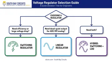
TI uses exactly this hybrid pattern on its data-acquisition reference designs, pairing DC-DC modules with LDOs on sensitive ADC supplies.
Whichever you choose, read the datasheet's recommended dropout voltage and output capacitor values before you start placing parts. Layout decisions downstream depend on both.
Essential PCB Power Supply Layout Design Tips
Once the regulator topology is set, layout execution determines whether the design performs to spec or fights noise and heat for its entire service life.
Grounding and Power Plane Strategy
On multilayer boards, dedicate solid ground and power planes rather than routing power as traces. Solid copper pours lower impedance and reduce voltage drops across the board.
- Isolate power ground from system ground, connecting them at a single point to prevent ground loops
- Separate noisy digital/switching zones from analog ground areas — mixing them lets switching noise couple directly into sensitive feedback or measurement circuits
- Treat the ground plane as part of your current return path, not just a reference. Return current follows the path of least impedance, typically directly beneath the trace above it
Trace Width and Copper Thickness
With grounding handled, power traces should be as short and wide as physically possible. Where board space allows, use copper pours or polygons instead of thin traces for any high-current path.
- Calculate minimum trace width using the IPC-2152 standard, which sizes conductors by current, temperature rise, copper weight, and layer position instead of relying on outdated single-variable rules of thumb. See IPC's current-carrying capacity standard for the full methodology.
- Standard 1oz copper works fine for low-current logic and control signals
- 2oz copper or heavier reduces resistance and heat buildup on higher-current power paths, though it does add fabrication cost
Component Placement and Capacitor Strategy
Trace sizing addresses resistive losses; placement determines transient response. Place the regulator, its input/output capacitors, and any inductor as close together as physically possible. Every millimeter of extra trace length adds parasitic inductance that degrades transient response.
- Put 0.1 µF decoupling capacitors directly at each IC's power pins, connected with short traces or vias straight into a low-impedance ground plane
- Position output capacitors near the regulator output pin to catch voltage overshoot when the load changes suddenly
- Keep heat-generating components physically separated from temperature-sensitive parts like feedback resistors and voltage reference circuitry
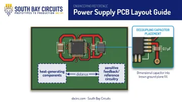
A capacitor placed even a centimeter too far away introduces enough trace inductance to undermine its ability to suppress switching noise. This is one of the most common and most fixable layout mistakes on power boards.
Thermal Management and EMI Control Techniques
Heat and noise are the two failure modes layout is best positioned to prevent. Both respond to the same underlying discipline: keep current paths short, and give heat somewhere to go.
Thermal control:
- Add thermal vias under regulator exposed pads to move heat from top copper into inner or bottom layers
- Use copper pour as a heat spreader; copper area affects thermal performance more than a single package's theta-JA rating once real airflow conditions apply
- Add a heatsink for any regulator dissipating more than a watt or two in an enclosed space
EMI control, in priority order:
- Minimize the current loop area first — this is the single biggest EMI lever available at layout time
- Use a ground plane between signal and power layers to shield high-frequency currents
- Add an input EMI filter if long conductors still carry high-frequency switching current after loop area is optimized
- Use shielded inductors and careful switching-node placement to reduce magnetic and electric-field coupling
Component placement and loop geometry changes alone can materially reduce conducted and radiated emissions in DC-DC designs. Filtering works best as a backstop once the loop area is already tight; it doesn't replace careful placement to begin with.
Before sending Gerbers to fabrication, run a thermal or power-integrity simulation. It's far cheaper to move a via pattern in CAD than to discover a hotspot on a populated board. Design teams that build a DFM review into the process, such as South Bay Circuits' pre-fabrication checks, catch these thermal and EMI risks before layout ever leaves CAD.
Circuit Protection, Voltage Handling, and Common Mistakes to Avoid
Can a PCB handle 12V? Yes, and considerably higher, as long as trace width, copper thickness, and dielectric spacing are sized for the actual voltage and current involved. There's no universal voltage ceiling in the IPC standards: spacing requirements scale with voltage, conductor location, and coating, not a fixed number.
Voltage ratings only cover normal operation. The board also needs protection components sized for fault conditions, not just nominal use.
Protection components to plan for:
- Fuses and circuit breakers guard against overcurrent conditions before they cause thermal damage
- TVS diodes absorb voltage spikes, but selection requires matching breakdown voltage, clamping voltage, and pulse-power rating to the surge profile and the protected component's ratings
- Input filters and regulators smooth out line noise before it reaches sensitive downstream circuitry
Protection components alone can't offset fundamental layout errors.
The mistakes that send boards back for a respin:
- Undersized trace widths cause excessive voltage drop and localized heating that only surface under real load, not bench testing
- Decoupling capacitors placed too far from IC pins: the added trace inductance quietly defeats their entire purpose
- Skipping thermal or power-integrity simulation: issues caught in CAD cost minutes to fix; the same issues caught on a populated board cost a full fabrication cycle
Every one of these mistakes is preventable at the review stage, before a board ever reaches a fabricator.
Work With an Experienced PCB Partner From Design to Assembly
Layout mistakes on power supply boards are far cheaper to catch on screen than on a populated prototype. That's the argument for working with a manufacturer that reviews layout for manufacturability before fabrication starts, rather than one who simply builds whatever file you send.
South Bay Circuits has operated as a single-source PCB design, fabrication, and assembly manufacturer since 1981, running design, 24-hour fabrication, and same-day assembly out of one 60,000-square-foot facility in Chandler, Arizona.

That in-house structure matters specifically for power supply boards. Grounding strategy, trace width, and thermal layout issues get flagged while the design is still a file, not after copper has been etched.
SBC's process runs under:
- ISO 9001:2015 certification for quality management
- AS 9100 compliance for aerospace applications
- ISO 13485 compliance for medical device electronics
- ISO/TS 16949 compliance for automotive programs
For teams designing power conversion boards headed into regulated aerospace, medical, or automotive programs, that combination of in-house control and industry-specific compliance reduces the back-and-forth that typically stretches out a design cycle.
If you're working through a power supply layout and want a second set of eyes before committing to fabrication, reach out to South Bay Circuits to talk through the design.
Frequently Asked Questions
What is a power supply PCB?
It's the board circuitry responsible for converting and regulating incoming AC or DC power into the stable voltages onboard components need. It typically involves multiple conversion stages, from AC-DC rectification down to low-noise linear regulation.
Can a PCB handle 12V?
Yes. Standard PCBs handle 12V and considerably higher when trace width, copper thickness, and dielectric spacing are correctly sized for the voltage and current involved, following IPC spacing guidelines.
What is the difference between linear and switching power supply PCBs?
Linear regulators produce very low noise output but waste excess voltage as heat, making them inefficient for large voltage drops. Switching regulators achieve much higher efficiency but introduce switching noise that requires EMI mitigation.
How do you reduce EMI in a power supply PCB layout?
Start by minimizing the high-current loop area and adding a ground plane between power and signal layers. Add input EMI filters and shielded inductors only if noise persists after the loop geometry is optimized.
Why are decoupling capacitors important in PCB power design?
They suppress voltage fluctuations and switching noise right at the IC power pin, where impedance matters most. Trace inductance from placing them too far away undermines that effectiveness.
How thick should copper be for a power supply PCB?
Standard 1oz copper works for low-power circuits and control signals. Higher-current paths typically need 2oz copper or heavier to keep resistance and heat rise within acceptable limits.