Introduction
SMT prototype assembly mounts surface-mount components onto a small batch of bare PCBs so you can build and validate a working circuit before full-scale production. This is where a schematic and BOM either prove out—or expose problems that cost far more to fix after tooling and volume builds begin.
If you're a hardware engineer, NPI lead, or product developer in medical, aerospace, automotive, or industrial electronics, you already know the pressure: a functional board fast, without trading away reliability. This guide is your roadmap.
"Prototype assembly" gets used loosely in conversation. The sequence of steps, equipment, and checkpoints is what determines whether a first-run board works. This article breaks down each step, the factors that shape outcomes, and when it makes sense to bring in a specialized partner.
Key Takeaways
- SMT prototype assembly uses the same core sequence as production—compressed into smaller batches and tighter timelines
- Stencil design, placement accuracy, and reflow profiling directly determine first-pass yield
- Manual vs. automated placement depends on component complexity, quantity, and how fast the design needs to scale
- A single-source assembler reduces handoff delays and rework risk during NPI
What Is SMT Prototype Assembly (and Why It Matters)?
SMT prototype assembly means mounting surface-mount components onto a small quantity of bare PCBs to create working boards for design validation, ahead of a full production run. The goal is a functional, testable board that proves the design works and surfaces manufacturability issues before they get expensive.
It differs from full production SMT assembly in a few key ways:
- Smaller quantities and faster turnaround
- Flexibility for design revisions over high-volume tooling
- Lines built to absorb change, not repeat one board thousands of times
Why SMT Prototype Assembly Matters for Product Development
This stage validates functionality and catches design errors (footprint mismatches, thermal issues, part conflicts) before you've committed to large component orders or hard tooling. Product development at this phase demands three things:
- Speed to keep the schedule moving
- Flexibility to swap components or revise layout between iterations
- Confidence the design will scale cleanly into volume production
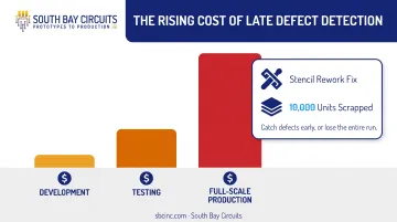
The cost of skipping this step is well documented. Siemens' NPI guidance for PCB development notes that the cost of fixing a design issue increases roughly tenfold at each stage from development to testing to full-scale production.
A footprint error caught during prototype assembly might cost a stencil rework. The same error after a 10,000-unit run costs far more: scrapped boards, missed launch dates, and lost customer trust.
That is why fast-turn capacity exists for this stage. South Bay Circuits, for example, offers same-day assembly and design-to-loaded-board turnaround as fast as 48 hours when design and layout are finalized, so validation does not wait weeks for a production slot.
How the SMT Prototype Assembly Process Works (Step-by-Step)
The process moves a bare PCB and sourced components through paste application, placement, reflow soldering, and inspection to arrive at a tested, functional assembly, typically within days rather than weeks.
Inputs: design/Gerber files, the BOM, solder paste, and components. Output: a validated, working board ready for the next design iteration or production scale-up.
Step 1: PCB Design Review & DFM Check
Before anything touches a stencil, engineers review the design against design-for-manufacturability (DFM) guidelines. That means checking footprints, pad spacing, and fiducial marks to prevent placement or soldering defects downstream. IPC-7351 and IPC-2221 provide the land-pattern and design standards most assemblers reference here.
Alongside the layout review, teams finalize the BOM and cross-check it against the design files. Prototype runs come with their own sourcing headaches:
- Low minimum order quantities from distributors
- Package size verification for every listed part
- Long-lead or unique components that create schedule risk if not flagged early
South Bay Circuits addresses this with its own manufacturability guidelines for both PCB fabrication and assembly, applied during early engineering review, before layout is locked in.
Step 2: Solder Paste Application
Solder paste goes on through stencil printing: the stencil is aligned to the board, and a squeegee pulls paste across the apertures. Deposit volume directly affects joint quality. Too little paste starves the joint; too much invites bridging.
Aperture design matters more than most people expect. An IPC technical study found that most solder pastes achieve acceptable transfer efficiency above an aperture area ratio of 0.66, while ratios below 0.50 commonly produce unacceptable results. Squeegee pressure needs to stay light, just enough for a clean wipe, since excess pressure shifts the stencil and wears down small apertures over time.
Once printed, operators check paste deposits manually or with automated solder paste inspection (SPI) before the board reaches placement.
Step 3: Component Placement
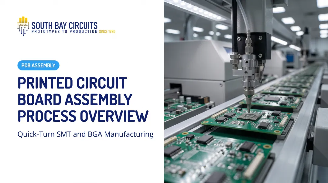
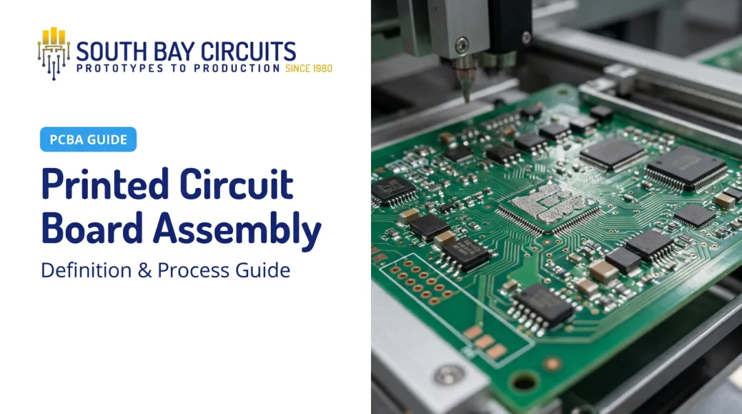
For most prototype builds, vision-guided pick-and-place machines place components using fiducial alignment to keep everything registered accurately. Very small prototype quantities — think one to five boards with unusual parts — sometimes call for manual placement with tweezers instead, especially for components not yet packaged in tape-and-reel.
Before running the full board, technicians verify machine programming against the BOM and design data. Skipping this check is a common (and costly) way to place the wrong part in the right spot.
Step 4: Reflow Soldering
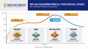
The board then moves through a multi-stage reflow profile: preheat, soak, reflow peak, and cooling. Each phase serves a purpose:
- Preheat: removes flux volatiles and limits thermal shock
- Soak: activates flux and evens out temperature across the board
- Reflow peak: forms the actual solder joint
- Cooling: locks in the joint's grain structure
Getting this profile wrong causes real problems, especially on mixed-component prototype boards where thermal mass varies wildly between parts:
- Tombstoning: uneven heating pulls small passives upright as one solder pad wets before the other
- Cold joints: insufficient peak temperature or time above liquidus leaves a dull, weak connection
- Voiding: trapped gas creates gaps in BGA and QFN solder joints
Matching the profile to the paste alloy and component mix on the board is the difference between a working board and a respin.
Step 5: Inspection & Quality Control
Inspection catches what reflow might have gotten wrong. Manual microscope checks handle small quantities and unusual defects. Automated optical inspection (AOI) scans for visible issues such as solder bridges, misaligned parts, insufficient solder, and lifted leads, often at multiple points in the process.
Visible defects are only part of the story. BGA and QFN packages hide their solder joints under the component body, which means X-ray inspection is required to verify hidden joint quality on these package types. South Bay Circuits keeps AOI and X-ray inspection in-house, alongside its Fuji SMT lines, so hidden defects are caught before a board reaches functional test, not after.
Catching problems here is far cheaper than catching them during powered testing, where a solder defect can masquerade as a design flaw and send an engineer chasing the wrong root cause.
Step 6: Functional Testing & Debugging
With inspection passed, technicians power up the board. Multimeters and oscilloscopes verify voltages, signal integrity, and functionality against the original design specs. This is where the board either proves the design or reveals what still needs work.
A systematic debugging approach matters here: check power rails first, then signal paths, then functional blocks, rather than probing randomly. Engineers document every issue found. That log becomes the input for the next design revision, not just a footnote.
Step 7: Documentation & Transition Toward Production
The final step is recording everything: BOM changes, assembly notes, and test results that build a traceable history for scale-up. This documentation is what separates a one-off prototype from a design that's actually ready to manufacture at volume.
A single-source manufacturer can carry that validated build directly into higher-volume production without re-qualifying a new vendor. South Bay Circuits' in-house design-through-production model is built for that handoff: the same team and equipment that ran the prototype can scale it, so nothing is lost between vendors.
Key Factors That Affect SMT Prototype Assembly Quality
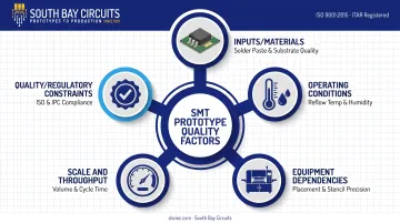
Several variables determine whether a prototype run comes out clean the first time or needs a second pass:
- Inputs/materials: Component package sizes (0402, 0201, and smaller), solder paste alloy type, and PCB surface finish quality all affect solderability and joint consistency
- Operating conditions: ESD controls, reflow oven calibration, and humidity levels; humidity in particular affects how paste behaves during printing and reflow
- Equipment dependencies: Stencil aperture design, pick-and-place accuracy, and whether AOI or X-ray inspection is available in-house
- Scale and throughput: Number of unique parts, panel size, and whether the batch size fits manual or automated placement better
- Quality/regulatory constraints: Industry requirements such as ISO 13485 (medical), AS 9100 (aerospace), or IPC-6012 Class III, which raise inspection rigor and documentation demands
These constraints aren't just paperwork. A defense program requiring IPC-6012 Class III inspection will demand more rigorous solder joint acceptance criteria than a commercial industrial board, which changes how much time and attention each step in the process gets.
Common Issues and Misconceptions in SMT Prototype Assembly
Misconception #1: Prototype assembly is just production assembly at a smaller scale.
It isn't. Tooling, machine programming, and vendor flexibility differ meaningfully between the two. A production line is optimized for repeating one job thousands of times; a prototype line needs to pivot between jobs constantly.
Misconception #2: Passing inspection means the design works.
There's a real difference between "assembled" and "working." A board can be fully soldered, pass AOI and X-ray with zero defects, and still fail functionally because of a design error: a wrong resistor value, a grounding issue, or a footprint that doesn't match the actual part.
Inspection validates the assembly process. It doesn't validate the design.
When full automated assembly might not be necessary:
- Extremely low quantities (1-5 boards)
- Highly experimental layouts still in flux
- Parts not yet available in tape-and-reel packaging
One signal worth watching: if a design keeps requiring multiple respins with an unstable BOM, full automated line assembly every time may be overkill. Manual assembly can save setup time and cost until the design settles. Full-line automation makes more sense once the BOM stabilizes and volume starts climbing.
Conclusion
SMT prototype assembly takes a design from files and loose components to a tested, working board: paste printing, placement, reflow, inspection, and functional testing. Each step builds on the last, and a shortcut in one stage tends to show up as a bigger problem two stages later.
Understanding this sequence matters most for engineers working under NPI time pressure. Small errors (a stencil aperture that's slightly off, a reflow profile that doesn't match the paste alloy) compound into costly redesigns if they slip through unnoticed.
Match the process to the design at each stage: manual or automated, in-house or outsourced. Choose the path that protects schedule and yield, not the one that looks most advanced on paper.
Frequently Asked Questions
What does SMT assembly mean?
SMT (Surface Mount Technology) assembly is the process of mounting electronic components directly onto the surface of a PCB, rather than through drilled holes. It enables smaller, denser boards that assemble faster than through-hole designs.
What is an SMT assembly line?
It's a connected sequence of machines that move a PCB through each assembly stage in order, from bare board to finished assembly. The line typically includes a solder paste printer, pick-and-place machine, reflow oven, and inspection systems.
What is an SMT assembly operator?
An SMT assembly operator sets up, runs, and monitors the equipment throughout the line. That includes loading component feeders, programming placement machines, and checking paste and solder quality at each stage.
How long does SMT prototype assembly typically take?
Turnaround depends on component sourcing and board complexity. South Bay Circuits offers same-day and multi-day quick-turn prototype builds, far shorter than the weeks typical of full production scheduling.
How many boards are typically included in a prototype assembly run?
Prototype runs are usually small batches, anywhere from a handful of units up to 50 or 100 boards. That's typically enough to validate the design before committing to a larger production order.
What's the difference between SMT prototype assembly and full production assembly?
Prototype assembly prioritizes speed and flexibility for design validation on small quantities. Production assembly is optimized for consistency, cost efficiency, and throughput once the design is locked in and ready to scale.