What separates a "high-current" board from a standard signal board isn't a fixed amperage number. It's the point where power dissipation, thermal rise, and conductor spacing become primary design drivers instead of afterthoughts.
This guide covers the core layout guidelines, trace and copper sizing, thermal management, grounding, along with the safety considerations, clearance, overcurrent protection, and certifications, needed to build reliable, compliant high-current boards.
Key Takeaways
- Size traces, copper weight, vias, connectors, and grounding as one system—not in isolation.
- Plan thermal management during component placement, not after routing.
- Spacing, overcurrent protection, and connector ratings drive shock and fire risk.
- Regulated-industry manufacturing experience lowers non-compliance and reliability risk.
Trace Width, Copper Weight, and Current-Carrying Capacity
Trace sizing for high-current boards starts with IPC-2152, the standard that governs current-carrying capacity in printed board design. It factors in continuous current, acceptable conductor temperature rise, board thickness, copper thickness, and how nearby planes or vias affect heat dissipation. IPC-2152 sizes internal and external conductors based on these combined thermal and electrical variables, rather than current alone.
A simplified example: if a trace needs to carry 8A with a 20°C allowable rise on an external layer, you'd reference the IPC chart for cross-sectional area, then convert that to a trace width based on your copper weight. Internal layers need noticeably more copper area than external layers for the same current, since internal copper dissipates heat only through the board material rather than open air. Those thermal limits force a practical choice when real estate is limited.
Trace Width vs. Copper Weight
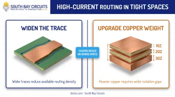
When board space is tight, you have two levers:
- Widen the trace — simple, but eats into routing density fast.
- Upgrade copper weight (1 oz to 2 oz or 3 oz) — saves space but changes your minimum trace/space rules and etching tolerances.
Heavier copper etches less precisely, so fabricators need wider isolation gaps to compensate. Most shops handle 2 oz copper with standard processes; some go further. South Bay Circuits, for example, lists 3 oz as its maximum starting copper foil weight before plating, with 2 oz trace/space capability down to 0.010"/0.010" on standard technology.
Vias and Copper Pours
A single via at a layer transition can become a hotspot fast. Current density spikes at that one connection point.
For high-current paths, plan the copper path—not just the trace:
- Place via arrays near power pads, MOSFETs, and connectors to spread load across parallel paths and cut voltage drop
- Prefer copper pours or dedicated power planes on backplanes and other low-voltage/high-current distributions instead of discrete traces
- Check thermal-relief spokes at through-hole pads; a narrow spoke can choke current as badly as an undersized trace
Rule of thumb: start with a trace-width calculator, then add a 15–20% derating margin. Calculator minimums assume ideal conditions your enclosure probably won't provide.
Thermal Management Techniques for High-Current PCBs
Heat in high-current boards comes from three main sources: copper resistance (I²R losses), connector contact resistance, and undersized vias. It rarely shows up during quick bench tests. Problems appear after sustained full-load operation, which is exactly why thermal planning can't wait until after routing.
Thermal Via Placement and Copper Pours
Place thermal vias directly under hot components and pads to create a low-resistance path to heat-spreading copper or opposite-layer planes. According to Texas Instruments thermal design guidance, maximize via count under exposed thermal pads with roughly 1mm spacing, connected to as many copper layers as possible.
Copper pours matter too. TI's thermal guidance notes that a typical two-sided board with solid copper fill needs at least 15.29 cm² to dissipate 1W with a 40°C rise under natural convection. Internal ground planes on a four-layer board can improve thermal performance by up to 30% compared to a well-designed two-layer board.
Material Selection
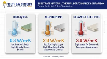
Not every high-current board needs exotic substrates, but for demanding duty cycles or tight enclosures, material choice matters:
| Substrate | Thermal Property | Best Use Case |
|---|---|---|
| High-Tg FR4 (e.g., Isola FR408HR) | Tg 190°C, 0.4 W/m·K | Multilayer boards needing thermal reliability |
| Aluminum IMS | 5-10x FR4's thermal conductivity | Single-layer, high-heat industrial/automotive circuits |
| Ceramic-filled PTFE (e.g., Rogers TC350 Plus) | 1.24 W/m·K | Defense, aerospace, industrial heating applications |
For bulky components like large inductors or heat sinks, a thicker board (2-3mm) adds both mechanical support and thermal mass. This isn't universal. Standard board thickness ranges run roughly 0.020" to 0.230", and the right choice depends on the specific load and enclosure.
Before committing to production, run thermal simulation during layout, then confirm with thermal camera or thermocouple testing under real load. Simulations catch obvious problems; physical testing catches the ones simulations miss.
Grounding, Power Planes, and EMI Control
Grounding Strategy for Power Systems
High-speed signal boards avoid split ground planes almost universally. High-current power boards work differently. Intentional ground segmentation—separating AC input, unregulated DC, and regulated DC sections—is often necessary to keep noise in one section from corrupting another.
An isolated grounding strategy becomes mandatory whenever primary and secondary sides of a power supply need galvanic isolation for operator safety, not just noise control.
For power delivery, use solid copper planes or wide pours sized for continuous and peak current. Keep the return path directly under the power path so loop inductance stays low and voltage drop stays predictable.
Minimizing EMI Without Sacrificing Power Delivery
Keep high-current loop areas short. Place input capacitors, switching devices, and loads close together to limit radiated noise—without narrowing the actual power path.
Three practical habits help:
- Place decoupling capacitors as close as possible to switching components
- Stitch vias along ground plane edges to hold continuity and limit local voltage differentials
- Keep high-current returns on adjacent layers under the power path to shrink loop area
These steps cut EMI without starving the copper you need for current capacity.
Safety Considerations in High-Current PCB Design
Safety in high-current design isn't a checklist item you add at the end. It shapes trace spacing, component selection, and protection strategy from the first layout pass.
Conductor Spacing and Clearance
IPC-2221's voltage-to-spacing tables define the creepage and clearance distances needed between conductors to prevent arcing or dielectric breakdown. Higher voltages demand more physical separation, and this scales with altitude, pollution degree, and insulation type under standards like IEC 60664-1.
Overcurrent Protection
Fuses, circuit breakers, and PTC devices limit fire risk when a trace or component fails under fault conditions. Littelfuse recommends sizing fuses to operate at no more than 75% of nominal current at 25°C. Voltage rating and breaking capacity should both exceed the circuit's requirements. PTC devices follow a similar logic. Eaton recommends at least 20% hold-current margin at room temperature.
Insulation, Connectors, and ESD
- Use isolated grounding between primary and secondary sides of power supplies to protect operators from shock
- Choose safety-certified connectors (UL 1977, for example) with margin above expected current and voltage—contact resistance is a frequent hotspot
- Place ESD circuitry near sensitive components; high current does not make nearby logic immune to static damage
Compliance requirements shift by industry:
- Medical: IEC 60601-1
- Automotive: IATF 16949 process requirements
- Aerospace: AS9100
- General equipment: IEC 62368-1 or IEC 61010-1
Build to the recognized standard for your market from day one to avoid costly redesigns later.
Component Selection, DFM, and Choosing the Right Manufacturing Partner
Component Selection Fundamentals
MOSFETs, inductors, and connectors all need current rating, thermal resistance, and safety margin evaluated together, not in isolation. Ignore the margin and you get long-term failure: a connector rated exactly at expected current will run hot indefinitely and degrade faster than one with headroom.
DFM Guidelines for Heavy Copper
Heavier copper weights change your manufacturability math:
- Minimum trace-to-edge spacing increases with copper thickness.
- Drill-to-copper clearance needs extra margin to avoid shorts during etching.
- Isolation gaps widen as copper weight goes up, since etching removes copper both downward and sideways.
These aren't universal numbers across every fabricator. They vary by shop and process, which is exactly why an engineering review of your specific stack-up matters before finalizing a layout.
Choosing a Manufacturing Partner
High-current, safety-critical designs benefit from a single-source partner controlling design, fabrication, and assembly under one roof. Fewer handoffs mean fewer opportunities for a file mismatch or process gap to turn into a field failure.
South Bay Circuits has operated this way for more than 40 years from its 60,000 sq ft Chandler, Arizona facility. The company holds ISO 9001:2015 certification, AS 9100 aerospace compliance, ISO 13485 medical compliance, and ISO TS 16949 automotive compliance.

Those credentials cover the regulated industries where high-current design mistakes carry the highest consequences, and support projects from initial layout through production without switching vendors mid-project.
Frequently Asked Questions
What is considered a high-current PCB?
There's no single amperage threshold. A board qualifies as "high current" once current flow becomes a primary driver of trace width, copper weight, and thermal design rather than a secondary concern.
How do I calculate the right trace width for a high-current design?
Use the IPC-2221/IPC-2152 formula, which factors in current, allowable temperature rise, and copper thickness. Add a safety margin beyond calculator minimums rather than relying on the bare result.
Is 1 oz copper enough for high-current PCB design?
It can work for short, wide, low-duty-cycle paths. Higher sustained currents in enclosed products typically need 2 oz or 3 oz copper to manage heat rise adequately.
Can vias safely carry high current?
A single via has limited current capacity and can become a hotspot at layer transitions. Use via arrays near power pads, MOSFETs, and connectors to spread current across multiple parallel paths.
What safety standards apply to high-current PCB design?
IPC-2221 governs conductor spacing, UL certifications apply to components and connectors, and industry-specific standards like IEC 60601-1 (medical) or IATF 16949 (automotive) add further requirements.
What certifications should I look for in a high-current PCB manufacturer?
Look for ISO 9001, AS9100, ISO 13485, and IATF/TS 16949, depending on your target market. These indicate a manufacturer's process controls for reliably producing boards for regulated, safety-critical industries.