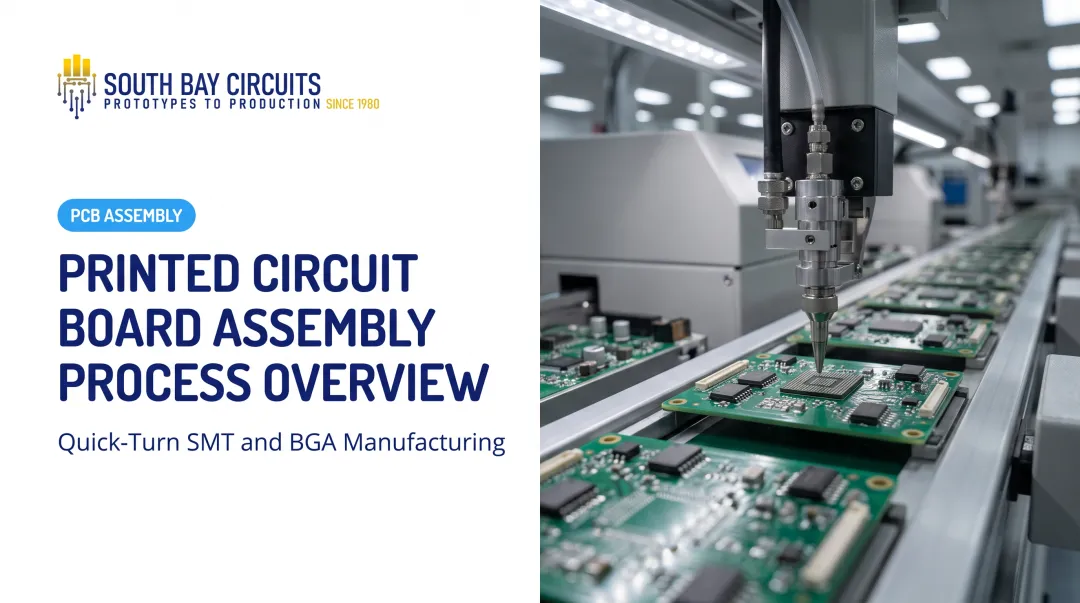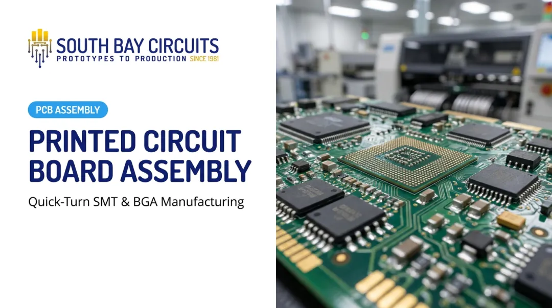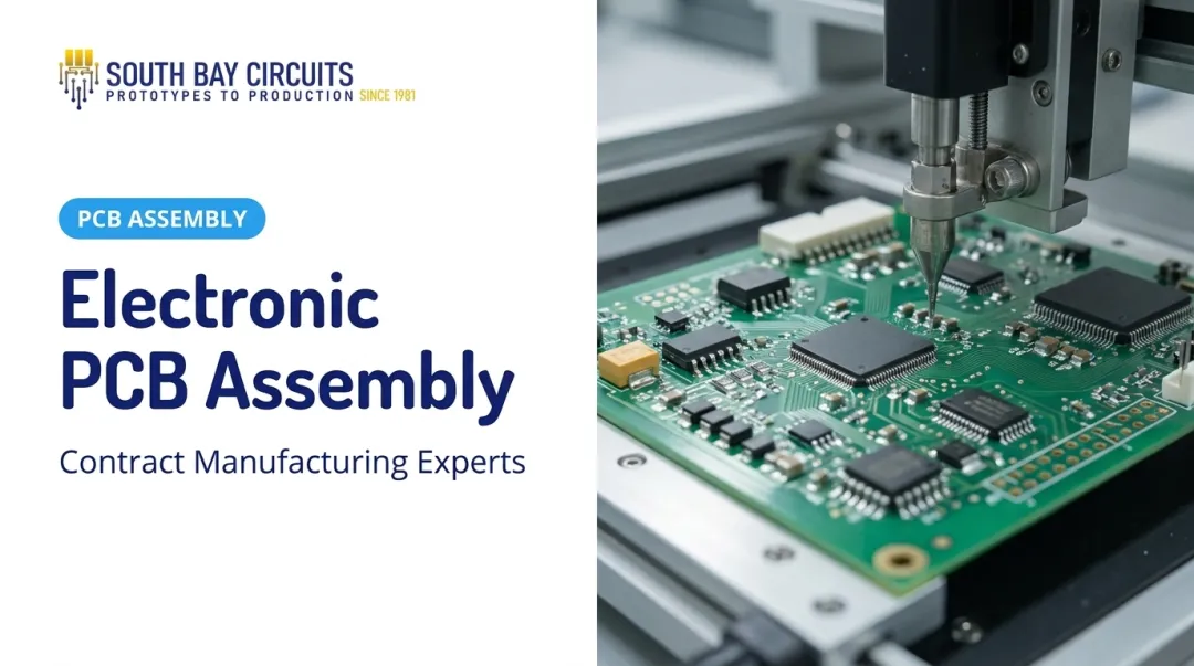
Here's a common problem: "PCB assembly" gets used interchangeably with "PCB fabrication," even though they're separate manufacturing stages with different inputs, equipment, and risks. This article breaks down how the assembly process actually works, what factors shape the outcome, and where it applies across different production scenarios.
Key Takeaways
- PCB assembly (PCBA) adds components to a bare board; board fabrication is a separate, earlier step
- The process follows a set sequence: DFM review, paste application, placement, soldering, and inspection
- Component density, board complexity, and certifications like ISO 13485 or AS9100 shape the process
- The right assembly partner and process controls prevent costly defects in regulated industries
What Is the PCB Assembly Process?
PCB assembly, often shortened to PCBA, is the stage where electronic components (resistors, integrated circuits, connectors, capacitors) are mechanically and electrically attached to a bare printed circuit board. Once complete, an inert piece of laminate with copper traces becomes a working circuit capable of powering and running an electronic device.
PCB fabrication and PCB assembly are not the same service, though the terms get mixed up constantly:
- Fabrication creates the bare board: copper traces, layer stack-up, drilled holes, substrate, and solder mask
- Assembly takes that finished bare board and populates it with the components that make it functional
- Together, they complete the manufacturing path from raw substrate to a finished, functioning board
Fabrication builds the board's structure. Assembly turns it into a functioning circuit.
Why the PCB Assembly Process Is Critical in Electronics Manufacturing
Demand for contract electronics manufacturing keeps climbing. The global electronics manufacturing services market is projected to grow from $648.51 billion in 2025 to $853.05 billion by 2030, a 5.6% CAGR, according to MarketsandMarkets. That growth reflects a broader shift: more products depend on precisely assembled electronics, not fewer.
Component Complexity Demands Precision
Modern boards pack fine-pitch ICs, ball grid arrays (BGAs), and micro-passives into shrinking footprints. Infineon's own board assembly guidance for wafer-level BGA packages covers 0.4mm and 0.5mm ball pitches.
Vision-equipped automated placement equipment achieves accuracy of ±50 micrometers or better, a tolerance a human hand simply cannot replicate consistently. At that scale, automated placement is the only reliable way to hit spec on every board.
Regulated Industries Add Another Layer
Medical, aerospace, and automotive OEMs need more than functional boards. They need documented, traceable processes:
| Standard | Governs |
|---|---|
| ISO 13485 | Medical device quality management systems |
| AS9100 | Aviation, space, and defense supply chain QMS |
| IATF 16949 | Automotive QMS, including traceability requirements |
These frameworks control documentation and process discipline; workmanship itself is governed by IPC standards like J-STD-001 and IPC-A-610.
What Goes Wrong Without Discipline
Skip the controls and you get cold solder joints, misaligned components, and tombstoning. ASQ's cost-of-quality framework breaks failure costs into four buckets: prevention, appraisal, internal failure, and external failure. External failures like warranty claims and returns typically cost far more than catching the same defect on the line.
A defect caught during inspection is a line adjustment. The same defect found in the field is a recall, a warranty claim, or worse.
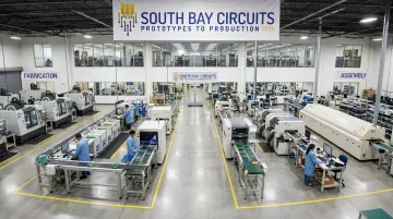
This is where single-source manufacturing changes the equation. When one facility controls design, fabrication, and assembly under one roof, there's no hand-off between vendors where responsibility gets murky.
South Bay Circuits, for example, positions its integrated Chandler, Arizona operation around exactly this idea: eliminating the "blame game" that shows up when fabrication and assembly are outsourced to separate companies with separate quality systems.
How the PCB Assembly Process Works (Conceptual Flow)
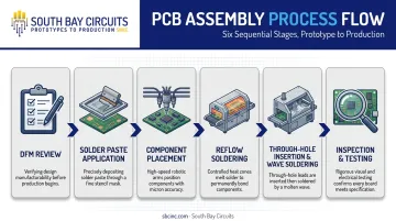
At a high level, a bare board moves through paste application, component placement, soldering, and inspection in a tightly sequenced, largely automated line. The inputs are consistent regardless of product type:
- A bare, fabricated PCB
- A bill of materials (BOM)
- A pick-and-place program
- Solder paste and flux
Process control comes down to three variables: temperature profiles during reflow, placement accuracy tolerances, and inline inspection checkpoints. Get these right, and an inert board becomes an electrically functional assembly ready for testing and integration.
Step 1: Design for Manufacturability (DFM) Review
Before anything hits the line, engineers review the board layout and BOM to catch problems early: placement conflicts, footprint mismatches, thermal issues that could cause defects downstream. This step catches expensive mistakes while they're still cheap to fix.
Step 2: Solder Paste Application (Stencil Printing)
A stainless-steel stencil deposits solder paste precisely onto the pads where surface-mount components will sit. Stencil design and paste transfer efficiency directly affect how consistently each pad receives the right paste volume.
Step 3: Component Placement (Pick-and-Place)
Automated pick-and-place machines position SMT components onto the pasted pads at high speed, guided by the placement program built from the BOM and board layout. For fine-pitch parts like 0.4mm BGAs, placement accuracy tolerances leave almost no room for error.
Step 4: Reflow Soldering
The populated board passes through a reflow oven with a controlled temperature profile — typically moving through preheat, soak, reflow, and cooling zones. This profile melts the solder paste just enough to form permanent electrical and mechanical joints without damaging components.
Step 5: Through-Hole Insertion & Wave Soldering
Larger components like connectors and electrolytic capacitors often need through-hole mounting for mechanical strength. When a board combines SMT and through-hole construction, these parts are inserted manually or mechanically, then soldered via wave soldering, selective soldering, or pin-in-paste reflow, depending on volume and part mix.
Step 6: Inspection and Functional Testing
Before anything ships, the assembly gets checked from multiple angles:
- Automated Optical Inspection (AOI) verifies component placement and solder joint appearance
- X-ray inspection checks hidden joints under BGAs and other bottom-terminated packages
- In-circuit and functional testing confirm the board actually performs as designed
Each test proves something different. A passed AOI scan confirms visual conformance, not electrical function. A board can look perfect and still fail under load. That's why in-circuit and functional testing exist as separate steps rather than a formality.
Where PCB Assembly Is Applied and What Affects the Process
Where the Process Is Applied
PCBA happens wherever electronic products need functioning circuits: consumer electronics, medical devices, aerospace avionics, automotive ECUs, and industrial control systems. Automotive transmission control modules, for instance, combine sensors and a high-temperature circuit board to manage sensing and wiring functions inside the vehicle.
Assembly happens at several points in a product's life:
- Prototype builds, to validate a design before committing to volume
- New product introduction (NPI), when a design moves toward production readiness
- Pilot runs, to confirm the process at small scale
- Full-scale production, for ongoing manufacturing
It's not a one-time event. Assembly repeats for every production run, batch, or design revision.
Key Factors That Affect the Process
Several variables shape how a given board gets assembled:
- Component types and package sizes: BGAs demand different placement tolerances and inspection methods than leaded components
- Board complexity and layer count: more complex boards affect line speed and how much inspection coverage is needed
- Equipment capabilities: pick-and-place accuracy and reflow oven zone count limit achievable component density
- Production volume and batch size: determine whether manual, semi-automated, or fully automated lines make sense
- Regulatory requirements: ISO 13485 for medical, AS9100 for aerospace, and ITAR for defense contracts add traceability and documentation on top of the core process. SBC holds all three, covering assembly work across those industries
Common Misconceptions and When the Standard Process May Need Adjustment
Common Issues and Misconceptions
A few assumptions cause real problems when they go unchallenged:
- "PCB assembly and fabrication are the same service." They're distinct stages, often handled by entirely different vendors with different equipment.
- "Faster turnaround always means lower quality." Not necessarily. Integrated single-source facilities can compress cycle time by eliminating inter-vendor delays, not by skipping quality steps.
- "Passing AOI means the board is reliable." Visual inspection confirms appearance. It says nothing about how the board performs under electrical load or environmental stress over time.
When the Standard Process May Need Adjustment
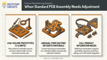
The standard automated flow isn't always the right fit:
- Extremely low-volume prototypes (1-5 units) rarely justify a full automated line setup. Manual or bench assembly usually makes more sense here.
- Unusual form factors or exotic materials (high-vibration aerospace applications, for example) may require custom fixturing or a hybrid manual/automated approach.
- PCB assembly alone doesn't cover full product integration. Box builds, cable and harness assembly, and system-level testing are separate but related services.
Understanding these distinctions, rather than defaulting to a one-size-fits-all vendor, helps OEMs choose the right automation level, certification, and turnaround for their specific application. South Bay Circuits, with over 40 years of in-house fabrication-to-assembly capability, built its model around this kind of flexibility. It helps customers avoid missteps that come from forcing every project through the same process.
Frequently Asked Questions
What is a PCB and why is it called that?
PCB stands for printed circuit board. The name comes from how conductive copper traces are "printed," or etched, onto an insulating substrate to connect components electrically.
What is the difference between a circuit board and a PCB?
"Circuit board" is a general term, while "PCB" specifically refers to a manufactured board with etched copper traces. This distinguishes it from older methods like point-to-point wiring or breadboard prototyping.
What is a PCB in an air conditioner?
In an air conditioner, the PCB acts as the control board. It manages compressor operation, reads temperature sensors, and regulates fan speed to keep the system running correctly.
What is the difference between PCB fabrication and PCB assembly?
Fabrication manufactures the bare board itself — copper traces, layers, and substrate. Assembly takes that finished board and populates it with components, turning it into a functional circuit.
How long does the PCB assembly process typically take?
Turnaround depends on complexity and volume. Quick-turn prototypes can ship in a day or two, while full production runs take longer. South Bay Circuits compresses these timelines by handling fabrication and assembly under one roof in Chandler, AZ.
What is the difference between SMT and through-hole assembly?
SMT mounts components directly onto the board surface, supporting higher density and faster automated assembly. Through-hole uses leads inserted through drilled holes, offering stronger mechanical bonds. Many boards use both.