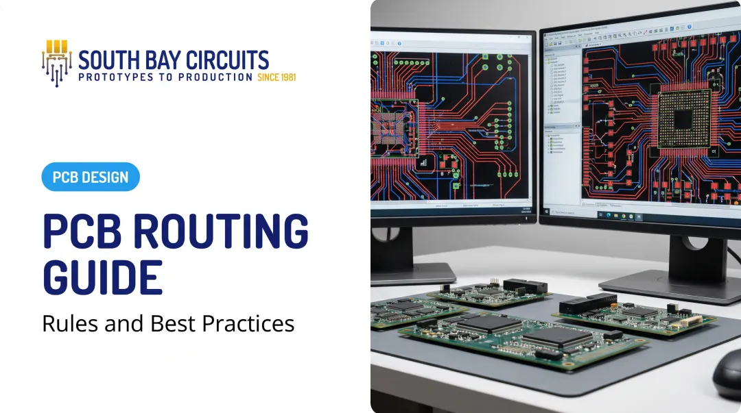
Routing looks simple in EDA software — click a pad, drag a line, connect the dots. But the results vary enormously depending on trace geometry, layer stack-up, component placement, and the type of signal running through each net. A power trace and a 10 Gbps differential pair have almost nothing in common once you get past "they're both copper."
This guide walks through the step-by-step routing process, the parameters that most affect outcomes, the mistakes that trip up even experienced designers, and when it makes sense to bring in a manufacturing partner for a design-for-manufacturing (DFM) review.
Key Takeaways
- Routing success depends on signal integrity, thermal performance, and manufacturability—not net connections alone
- Trace width, via placement, and plane continuity carry the biggest impact on long-term reliability
- Most routing failures start with skipped placement planning or too much trust in an autorouter
- A DFM review with an experienced fabricator catches errors design software misses
How to Route a PCB: Step-by-Step Best Practices
Good routing follows a sequence. Skip a step or do them out of order, and you'll end up reworking traces you thought were finished.
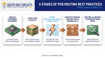
Step 1: Finalize Component Placement Before Routing
Placement decisions made now determine how clean or how painful your routing will be later.
- Group related components together (power circuitry, high-speed clusters, connectors) to keep critical traces short
- Confirm mounting holes, connector clearances, and keep-out zones before drawing a single trace
- Verify placement supports automated assembly access — tight component spacing near board edges can complicate pick-and-place
Step 2: Plan the Layer Stack-up and Ground/Power Planes
Your stack-up is the foundation everything else builds on.
- Assign dedicated, continuous layers for ground and power wherever the layer count allows
- Alternate signal layers with plane layers to control impedance and reduce layer-to-layer interference
- Keep the stack-up symmetric to reduce the risk of warping during fabrication Fabricators vary in how many layers they can reliably build. Confirm layer count, HDI options, and via types with your manufacturer early, especially if the design goes past a standard 4- or 6-layer stack-up. South Bay Circuits supports multilayer and HDI builds, so those limits are worth locking in before routing starts.
Step 3: Route Critical and High-Speed Signals First
Once placement and stack-up are locked, route the traces that matter most before anything else claims the board space.
- Route clock lines, differential pairs, and other high-speed nets first to secure their ideal paths
- Keep these traces short, direct, and routed over a solid reference plane
- Use 45-degree angles instead of sharp 90-degree bends to reduce impedance discontinuities and etching defects
Step 4: Complete General Routing, Vias, and Ground Fills
With the critical nets placed, fill in the rest of the board methodically.
- Route remaining signals with consistent spacing to prevent crosstalk, tightening tolerances only where board density demands it
- Place vias in a grid pattern rather than clustering them, and keep via-to-via spacing wide enough to avoid plane voids and current hot spots
- Add copper pours, thermal reliefs, and stitching vias for EMI shielding and heat dissipation before you finalize the layout
Step 5: Run Design Rule Checks and Compare Against Manufacturer Specs
DRC in your EDA tool catches clearance, spacing, and unconnected-net violations before release. But software checks against your own rule file — not necessarily against what your fabricator can actually build. Cross-check trace widths, via sizes, and clearances against your fabricator's minimum capabilities. As a reference point, South Bay Circuits documents .004"/.004" trace-and-space for standard technology, .003"/.003" with engineering review, and .002"/.002" on innovative-tier builds. Microvia diameters run from .006" down to .004" depending on tier. Catching mismatches at this stage pays off. Siemens reports that its Valor NPI DFM software can cut re-spins by an average of 57 percent (vendor-reported, not an independent industry average). Designs checked against real manufacturing limits before release still avoid far more rework than ones checked only against generic EDA defaults.
Key Parameters That Affect PCB Routing Results
Routing quality depends on several interacting variables, each with its own tolerance and failure mode.
Trace Width and Spacing
Why it matters: Trace width determines current-carrying capacity and resistive heating. Spacing determines vulnerability to crosstalk and shorts.
IPC-2152 governs conductor sizing against current and temperature rise, but it avoids a single universal ampacity table. The right width depends on copper thickness, layer position, and nearby planes.
Impact: Undersized traces overheat under load. Overly tight spacing invites signal coupling between adjacent nets.
Via Placement and Type
Blind vias connect an outer layer to inner layers without crossing the whole board. Buried vias connect internal layers only, never reaching either surface. Both free up routing area that through-vias would otherwise consume.
- Poorly placed vias create hot spots and plane voids
- Grid-pattern spacing keeps current distribution even
- Via type (through-hole, blind, buried) should match signal speed and density needs, not just habit
Impact: Wrong via type or placement wastes routing channels, weakens planes, and creates thermal and signal problems.
Differential Pair Symmetry and Length Matching
High-speed interfaces such as USB, HDMI, and Ethernet depend on matched timing and impedance between paired traces. There's no single universal mil value for acceptable mismatch; the allowance depends on rise time, dielectric constant, and the receiver's jitter tolerance.
For context, USB 2.0 on a two-layer board typically calls for keeping D+/D- mismatch within roughly 0.6 inches. Looser stripline layouts with slower rise times can tolerate far more.
Impact: Mismatched lengths or spacing cause skew, mode conversion, and reduced noise immunity.
Ground/Power Plane Continuity
At high frequency, return current follows the path of least inductance, typically directly beneath the signal trace. Slots, cutouts, and clearance holes interrupt that path, forcing return current to detour around the discontinuity and increasing loop area.
Impact: Split or interrupted planes cause long return-current detours, raising EMI risk and distorting signal integrity.
Common PCB Routing Mistakes to Avoid
Most routing problems trace back to a handful of repeat offenders:
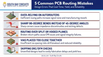
- Over-relying on an autorouter without manual review. Autorouters often produce inefficient, overly symmetrical paths that still need reworking
- Using sharp 90-degree bends instead of 45-degree angles. TDR tests found no measurable impedance change from right-angle bends, but sharp corners still risk etching defects and heat buildup
- Routing over split or voided planes, which breaks the return path and increases EMI susceptibility
- Placing vias too close to pads or each other, causing solder wicking and overlapping antipads
- Skipping DRC/DFM checks before release, which pushes avoidable errors into fab and assembly where fixes cost far more
Manual Routing, Autorouters, or Outsourced Layout: Choosing the Right Approach
The right method depends on board complexity, your timeline, and how much high-speed routing experience you have in-house.
Manual Routing
Best for high-speed, RF, or densely packed boards where every trace needs deliberate placement. It takes longer and demands more designer expertise, but it gives you tighter control over signal integrity than any automated tool currently matches.
Autorouter-Assisted Routing
Useful for simple, low-speed boards, or for handling bulk low-priority nets after critical paths are already placed manually. It's a faster first pass, but expect manual cleanup afterward. Early autorouters were notorious for layer bias and excessive via insertion, and modern tools still need a human check on the output.
Outsourced Layout or Design Support Services
Valuable when internal teams lack bandwidth or high-speed routing experience, or when a fast prototype-to-production timeline is on the line. This adds a vendor relationship, but an experienced PCB manufacturer's design team can align routing directly with real fabrication capabilities from the start.
South Bay Circuits, for example, offers in-house RF/microwave, high-speed digital, HDI, and power-electronics layout, with DFM and DFT verification built into the process rather than bolted on afterward. Layouts can turn in as little as 24 hours. Because fabrication and assembly happen in the same facility, boards can move from finished layout to supplied product in as little as 48 hours.
When to Loop In Your PCB Manufacturer for a DFM Review
Even well-planned routing benefits from a fabricator's perspective. Manufacturability issues such as tight annular rings, marginal impedance tolerances, and aggressive trace-to-space ratios aren't always visible from inside EDA software alone.
Request a manufacturer review early when your board involves:
- High layer counts or HDI construction
- Controlled-impedance requirements
- Tight tolerances where fabrication variance directly affects performance
Medical, aerospace, automotive, and military programs benefit most. Each carries certification demands (ISO 13485, ISO TS 16949, AS 9100, and ITAR with IPC-6012 Class III) that make a pre-production DFM check standard practice, not optional.
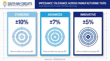
South Bay Circuits has supported OEM programs since 1981. Its design team reviews routing and stack-up files against real process limits: impedance tolerances of ±10% standard, ±7% advanced, or ±5% innovative, minimum drilled-hole spacing of .010", and controlled-impedance stack-up options.
That review catches clearance, via, and impedance issues while they are still cheap to fix, and it supports a faster path from design to loaded assembly.
A manufacturability problem found before fabrication costs a design revision. Found after, it costs a board re-spin and often the prototype-to-production schedule with it.
Frequently Asked Questions
What does routing mean in PCB design?
Routing is the process of laying out copper traces that physically connect components according to the schematic's electrical connections. It turns logical connections into a real, manufacturable board layout.
What is the 45-degree rule in PCB routing?
The 45-degree rule recommends angled bends instead of sharp 90-degree corners to reduce impedance discontinuities and lower the risk of manufacturing defects at trace corners.
How much spacing should be maintained between vias?
Spacing depends on your fabricator's capability and the voltage or impedance requirements involved. Always confirm the rule against your manufacturer's current capability table, especially in dense BGA regions.
Should I rely on an autorouter for my PCB design?
Autorouters can speed up simple or low-priority nets, but they shouldn't replace manual routing for high-speed, RF, or other critical signals where precise control matters.
Why shouldn't I route traces over a split ground plane?
Doing so breaks the signal's return path, forcing current to detour around the gap. That increases EMI risk and creates impedance discontinuities along the trace.
What is the benefit of a DFM review before fabrication?
A DFM review checks trace, via, and clearance details against real manufacturing capabilities rather than generic software defaults, catching issues that cause board re-spins and delays.