Introduction
Medical implants keep shrinking, aerospace avionics pack in more processing power, and automotive ECUs consolidate functions once spread across a dozen separate modules.
Medtronic's smallest pacemaker is now 93% smaller than earlier generations. Its implantable cardiac monitor now measures roughly one-third the size of a AAA battery, according to Medtronic's own miniaturization data.
None of that happens on a single-sided board.
Engineers face a real tension here. Cram more components onto a smaller footprint, and you introduce thermal risk, alignment headaches, and inspection blind spots. Pick the wrong assembly partner, and those risks turn into field failures.
This guide breaks down how double-sided SMT PCB assembly actually works, where it delivers real value, and where it gets tricky. It also covers how to choose a manufacturing partner capable of handling that complexity.
Key Takeaways
- Double-sided SMT doubles usable mounting area without growing the board footprint
- Two process routes exist: reflow-reflow, or adhesive-plus-wave for mixed-tech boards
- Second-side reflow puts existing solder joints at real risk of remelting or shifting
- Fine-pitch, high-density boards demand SPI, AOI, and X-ray inspection on both sides
- Medical, aerospace, and automotive sectors pair this method with certified quality systems
What Is Double-Sided SMT PCB Assembly?
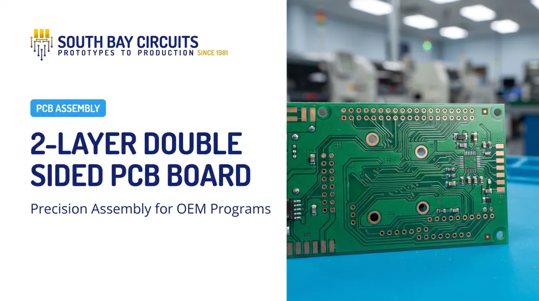
Double-sided SMT assembly places and solders surface-mount components on both faces of a printed circuit board, Side A (top) and Side B (bottom), with plated vias carrying electrical connections between the two layers.
| Aspect | Single-Sided SMT | Double-Sided SMT |
|---|---|---|
| Component placement | One face only | Both faces (Side A & B) |
| Board real estate | Baseline footprint | Effectively doubled |
| Layer connection | Not required | Plated vias link the layers |
The appeal is straightforward: usable board real estate effectively doubles without increasing the physical footprint.
That matters more every year. Medical Design Briefs notes that modern medical electronics now come in thumbnail-sized or smaller packages, with placement accuracy in some applications reaching +/-5 microns. Flip-chip/BGA combinations are shrinking to one-third or one-fourth the size of conventional BGA packages. These aren't proof that double-sided SMT alone drives the trend, but they show the density pressure engineers are designing against.
Why manufacturers reach for it:
- Fit more circuitry into a fixed or shrinking footprint
- Separate sensitive circuit types (analog vs. digital, RF vs. control) across faces
- Avoid the cost and complexity of adding board layers just for component count
The Double-Sided SMT Assembly Process: Step-by-Step
Two primary methods exist, and the right one depends on your component mix, production volume, and cost targets.
According to CircuitNet's technical panel, the most reliable way to think about double-sided SMT assembly is as two separate single-sided SMT processes run in sequence, not one combined operation. That framing matters because it explains most of the process controls below.
Method 1: Double Reflow Soldering (Most Common for Pure SMT Boards)
This is the standard route for boards populated entirely with surface-mount parts.
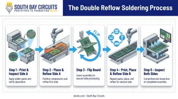
- Print and inspect Side A. Solder paste goes down through stencil printing, then Solder Paste Inspection (SPI) checks paste volume, height, and alignment before a single component gets placed.
- Place and reflow Side A. Pick-and-place equipment mounts components, then the board runs through a reflow oven to form solid joints.
- Flip the board. Fixtures or vacuum systems hold the board securely, protecting the now-soldered Side A joints during handling.
- Print, place, and reflow Side B. The same paste, placement, and reflow sequence repeats on the opposite face.
- Inspect both sides. AOI catches surface-level defects, while X-ray inspection checks hidden solder joints under BGAs and QFNs, where visual inspection simply can't see.
Here's the catch: Side A already has finished solder joints when Side B goes through reflow, and that second thermal cycle remelts Side A's solder.
A Cisco/Jabil study published in the SMTA Journal found BGA solder-separation defects appearing after second reflow, even on boards where some initial defects actually healed during that same cycle.
Manufacturers manage this by adjusting thermal profiles per side, accounting for component mass and board warpage, and validating support tooling before running production.
Method 2: Adhesive + Wave Soldering (For Mixed SMT/Through-Hole Boards)
This older, high-volume method suits boards combining through-hole and SMT components.
- Reflow solder Side A first, same as Method 1
- Secure Side B's SMT components with adhesive dots
- Pass the board through a solder wave, soldering Side B's through-hole leads and adhesive-retained SMDs simultaneously
- Protect Side A's finished joints from remelting, since wave soldering (not a second reflow) handles Side B
This approach works well for legacy mixed-technology designs. It's largely impractical for modern fine-pitch SMT layouts, though, since wave soldering carries a real bridging risk on tightly spaced pads.
Key Benefits of Double-Sided SMT PCB Assembly
Density and Design Flexibility
Using both faces increases available mounting area without growing the board. That's the core value proposition, and it's why the method shows up constantly in space-constrained categories like wearables and implantable medical devices.
It also opens design options that single-sided boards can't offer:
- Circuit separation: keep RF sections away from noisy digital circuits by placing them on opposite faces
- Signal integrity: shorter, more direct trace routing between layers reduces coupling risk
- Component isolation: physically separate heat-sensitive parts from heat-generating ones
Analog Devices' RF layout guidance backs this up structurally: keeping RF lines apart from high-speed digital signals, maintaining continuous ground planes, and controlling parallel-run distance all reduce coupling. Double-sided assembly gives engineers another axis, literally, to apply that separation.
Cost and Performance at Scale
That design freedom carries a real cost dimension at volume. Fitting more functionality onto fewer boards can reduce material and panel costs in medium-to-high-volume runs, though the actual savings depend heavily on your specific design, volume, and component mix. There's no universal percentage here worth quoting.
Consolidating two single-sided boards into one double-sided board also trims drilling, plating, and panel-handling steps in fabrication, each of which adds cost at volume. What stays consistent regardless of design: shorter trace lengths and tighter routing support faster signal timing, which matters directly for high-speed data buses and RF front ends.
Meeting Regulated-Industry Standards
Cost and speed matter, but regulated industries add another layer: compliance. Medical, aerospace, and automotive programs typically demand this density as a baseline requirement. But density without process control is a liability.
South Bay Circuits' ISO 13485, ISO/TS 16949, and AS9100 certifications, along with ITAR registration and IPC-6012 Class III capability, provide that process control for medical, automotive, aerospace, and military programs alike.
Common Challenges in Double-Sided SMT Assembly
Thermal Stress on Side A Joints
Every second reflow pass puts already-finished solder joints back into liquid state, often at peak temperatures near 245°C for lead-free assemblies. Component mass, thermal uniformity across the board, and warpage all influence whether those joints hold their position or shift, and a dense BGA on Side A can drift by a fraction of a millimeter if the board flexes during that second pass.
Mitigating that risk comes down to process discipline:
- Side-specific thermal profiles tuned for components already reflowed once
- Validated board-support fixtures that hold the panel flat during the second pass
- Warpage checks before the board ever enters the oven a second time
Component Placement and Clearance Conflicts
Thermal stress isn't the only risk from adding a second side: placing components on opposite sides close together creates real interference risk. A component footprint on Side B might conflict with a tall component's clearance zone on Side A, or with the fixture points needed to support the board during reflow, sometimes leaving less than 2mm of usable clearance for support pins.
This is squarely a Design for Manufacturability (DFM) problem:
- Underside components reduce available board-support locations during the second reflow
- Routed support plates with component cutouts improve repeatability, but add tooling cost and lead time
- Clearance reviews need to happen at the design stage, not after the first prototype run fails
Elevated Inspection Demands
Beyond placement conflicts, verifying the result on both sides raises the inspection bar. Double-sided boards need inspection on both faces, not just one, and misalignment fractions of a millimeter on fine-pitch components down to 0.4mm can cause open joints or shorts that AOI alone won't catch under a BGA or QFN package.
That's why a full inspection stack matters:
- SPI immediately after paste printing, before placement
- AOI after reflow, on both sides, for visible defects
- X-ray for hidden joints under ball-grid and fine-pitch packages
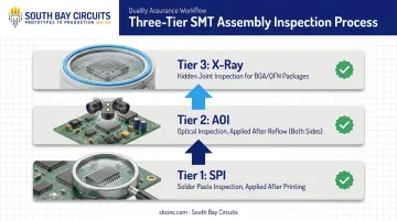
Skip any layer of that stack, and you're relying on final test to catch problems that should've been caught in-process.
Single-Sided vs. Double-Sided SMT: Which Is Right for Your Project?
Not every board needs both faces populated. The right call depends on complexity, budget, and where the product will live.
| Factor | Single-Sided SMT | Double-Sided SMT |
|---|---|---|
| Component density | Low to moderate | High |
| Typical use case | Basic controls, simple sensors | Medical devices, avionics, automotive modules |
| Process steps | One print/place/reflow pass | Two sequential passes, side-specific profiles |
| Cost driver | Fewer process steps, lower per-board cost | Higher per-process cost, potentially fewer boards needed |
| Inspection scope | One face to verify | Both faces, plus hidden-joint X-ray |
Choose single-sided when:
- The design has low component count and generous board space
- Cost sensitivity outweighs density requirements
- The end application doesn't demand tight tolerances
Choose double-sided when:
- Board space is genuinely constrained
- The product serves a regulated or high-reliability market
- Performance requirements (RF, high-speed digital) benefit from circuit separation
If you're unsure which side of that line your project falls on, that's exactly the kind of question our DFM review should answer before layout gets locked.
Why Partner with South Bay Circuits for Double-Sided SMT PCB Assembly
South Bay Circuits has run PCB fabrication and assembly under one roof since 1981. That single-source model, design through production without shipping boards between vendors, matters most on double-sided assemblies.
Every flip, re-solder, and inspection step adds a chance for something to go wrong between handoffs. Keeping design, fabrication, and assembly under one roof closes that gap.
Certifications that map directly to double-sided QC demands:
- ISO 9001:2015 — documented, controlled processes across the board
- AS9100 — aerospace-grade traceability and quality systems
- ISO 13485 — medical device compliance
- ISO/TS 16949 — automotive quality standards
Those aren't just badges. They're the same rigor that double-sided assembly's inspection stack, SPI, AOI, X-ray, requires to be trustworthy at scale.
That same rigor extends to geometry, too: SBC supports fine-pitch double-sided work down to 0.4mm pitch as a standard capability, with finer geometries available through engineering review. Standard BGA and Micro-BGA processing come with X-ray verification on every BGA assembly.
Speed matters here too. SBC offers 24-hour PCB fabrication and same-day assembly options, which shortens NPI cycles without cutting corners on the precision double-sided boards demand.
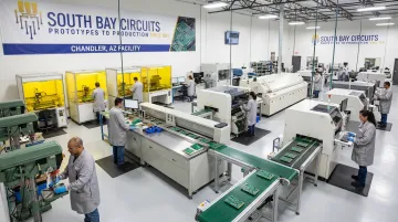
Design, fabrication, and assembly all happen at the same 60,000-square-foot Chandler, Arizona facility, so there's no multi-vendor blame game when something needs troubleshooting. One team owns the outcome.
Frequently Asked Questions
What is double-sided SMT assembly used for?
It's used for compact, high-density electronics where board space is limited but functionality demands are high. Medical devices, automotive control modules, and aerospace systems are the most common applications.
How long does double-sided PCB assembly typically take?
Timelines vary by board complexity, component mix, and production volume. Manufacturers like South Bay Circuits offer expedited options, including same-day assembly, for prototype and quick-turn production runs.
Is double-sided SMT assembly more expensive than single-sided assembly?
Per-board process costs run higher because of the added printing, placement, and reflow steps. At scale, though, total costs can come out lower since fewer boards are needed to deliver the same functionality.
Can double-sided PCB assembly include through-hole components?
Yes, mixed-technology boards are common. These typically use adhesive-plus-wave soldering, or selective soldering, to attach through-hole parts alongside SMT components on double-sided designs.
What industries rely most on double-sided SMT PCB assembly?
Medical devices, aerospace and defense, automotive, and industrial instrumentation lean on this method most heavily. Each sector needs compact, high-reliability electronics that single-sided boards can't deliver.
How is quality controlled during double-sided SMT assembly?
Manufacturers use SPI after paste printing, AOI after reflow on both sides, and X-ray inspection for hidden BGA and QFN joints. ISO-certified manufacturers add process documentation and consistency to that inspection stack.