Many engineers assume the rules that work for a 5V logic board scale up fine to 500V or 5kV. They don't. Clearance, creepage, material CTI ratings, and copper weight all behave differently once real voltage stress enters the picture.
The stakes are rising fast. Renewable power capacity grew by 473 GW in 2023 alone, a 13.9% jump in global installed capacity, according to IRENA's 2024 renewable capacity statistics. EV chargers, inverters, and industrial power supplies are pushing more boards into kilovolt territory than ever before.
This guide covers voltage thresholds, clearance and creepage rules, material selection, layout best practices, and the compliance standards that govern certification — plus how the right manufacturing partner reduces risk along the way.
Key Takeaways
- High voltage thresholds typically start at 30V RMS AC / 60V DC, per your governing standard
- Clearance and creepage spacing, not voltage ratings, set your board's real safety margin
- CTI rating, laminate type, and copper weight drive long-term reliability under stress
- IPC-2221, IEC 60664-1, and UL 796/61010 govern spacing, insulation, and certification
- A single-source design-to-assembly partner cuts compliance risk and speeds time to market
What Is a High-Voltage PCB?
A high-voltage PCB is a board engineered specifically to carry and isolate voltages that pose a genuine arcing or shock risk. The real difference from a standard board lies in the spacing, materials, and insulation strategy built around the voltage the board will actually see in service.
There's no single universal number that defines "high voltage" for a PCB. UL flags 30V RMS AC, 42.4V peak, and 60V DC as thresholds for Class 2 and limited-energy circuits, and several PCB design guides use these same figures to mark where layout treatment needs to change.
Treat these as design triggers, not a hard legal definition, and confirm the threshold that applies to your specific end product and certification path.
How Many Volts Can a PCB Handle?
There's no fixed ceiling here, no matter what a spec sheet headline suggests. A standard FR4 board with typical 6-mil spacing might handle a few hundred volts safely under clean, dry conditions. Push it further without adjusting spacing or materials, and arc risk climbs quickly, especially in humid or contaminated environments.
Properly engineered high-voltage boards tell a different story. With adequate clearance, the right laminate, and protective coatings, PCBs can safely manage voltages into the kilovolt range. The difference comes down to design discipline, not the base material alone.
IPC-2221's spacing methodology, for example, adds roughly 0.005 mm of clearance per volt above 500V for external, uncoated conductors. In practice, that means a 1,000V design needs roughly double the spacing of a 500V design, all else equal.
Common High-Voltage PCB Applications
HV PCB design shows up across a wide range of industries:
- EV powertrains and chargers — inverters and DC/DC converters commonly operate across 48V to 1,000V
- Industrial motor drives and power supplies — high current combined with elevated voltage
- Renewable energy inverters — solar and grid-tie systems requiring sustained voltage isolation
- Medical imaging and therapy devices — CT, mammography, and radiography systems
- Aerospace and defense systems — HV requirements layered with extreme environmental demands
- High-tech lasers and specialized research equipment — niche but growing applications
These applications map closely to industries governed by strict quality frameworks: industrial, medical, aerospace and defense, and automotive. That overlap is exactly why certified manufacturing expertise matters as much as the schematic itself.
Clearance and Creepage: The Foundation of High-Voltage Safety
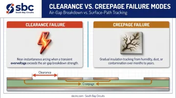
Two dimensions decide whether a high-voltage board survives in the field: clearance, the shortest through-air distance between two conductive parts, and creepage, the shortest path along an insulating surface between them. Both need independent verification during layout. Meeting one doesn't guarantee the other.
The failure modes differ too:
- Insufficient clearance causes near-instantaneous arcing when a transient overvoltage event exceeds the air gap's breakdown strength
- Insufficient creepage causes gradual insulation tracking as humidity, dust, or contamination carve a conductive path over months or years
What Determines Required Spacing
Several factors interact to set the minimum spacing your board actually needs:
- Peak working voltage, not just nominal or RMS voltage
- Pollution degree and the operating environment's cleanliness
- Altitude, since thinner air at elevation reduces dielectric strength
- Whether conductors sit internal or external, and coated or uncoated
Skipping any one of these factors can leave a design compliant on paper but vulnerable once it reaches a customer's operating environment. A board cleared at sea level, for instance, may arc at altitude despite passing every bench test at the factory.
The Comparative Tracking Index
The Comparative Tracking Index (CTI) measures a material's resistance to surface tracking failure, tested per IEC 60112 by applying repeated voltage drops until a specimen fails. UL groups materials into performance categories based on this test, as detailed in UL's Comparative Tracking Index resource:
| UL CTI Category | CTI Range (V) |
|---|---|
| 0 | ≥600 |
| 1 | 400 to <600 |
| 2 | 250 to <400 |
| 3 | 175 to <250 |
| 4 | 100 to <175 |
| 5 | <100 |
Standard FR4 typically lands in Category 3 (175–249V). That's fine for many applications, but it's a real limitation once you're pushing higher working voltages in dirty or humid environments.
Practical Mitigation Techniques
You don't always need a bigger board to fix a spacing problem:
- Route slots or cutouts between conductors to increase creepage distance without adding board area
- Apply conformal coatings to reduce effective creepage requirements
- Use vertical insulating barriers between high-voltage and low-voltage zones
For voltages above 500V, IPC-2221 Table 6-1 defines a base spacing plus a per-volt increment specific to conductor location and coating — the authoritative reference engineers should use rather than a rule of thumb.
Selecting the Right Materials for High-Voltage PCBs
Material choice determines how much margin your board actually has once it leaves the test bench and enters real-world conditions.
Laminate options differ in performance and cost:
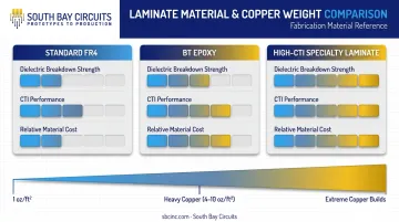
| Laminate Type | Strength | Trade-off |
|---|---|---|
| Standard FR4 | High dielectric breakdown | Weaker edge structure, vulnerable to contamination |
| BT epoxy | Strong sidewalls | Higher cost and more limited fabricator availability than standard FR4 |
| High-CTI specialty laminates | CTI ≥600V performance | Higher material cost |
Copper weight matters just as much as the laminate. Heavy copper (roughly 4–10 oz/ft²) and extreme copper builds (beyond that, depending on the fabricator's terminology) withstand the mechanical and thermal stress that comes with high current alongside high voltage.
Terminology varies by supplier, so confirm exact capability ranges before finalizing a design. South Bay Circuits fabricates across this full range, from standard 1 oz copper through extreme-copper builds, and verifies exact limits during DFM review.
A few additional details push performance further:
- Higher resin content and finer glass-weave styles improve dielectric properties, reducing weak points in the insulation
- Smooth surface finishes minimize arc paths across the board surface
- Conformal coatings (acrylic, urethane, or silicone) protect against moisture and dust ingress that would otherwise degrade creepage performance over time
Material selection also has to account for non-voltage stress. Aerospace and industrial HV applications often combine electrical demands with altitude, vacuum exposure, humidity swings, and temperature extremes, any of which can compromise a laminate that looks fine on paper.
High-Voltage PCB Design Best Practices and Compliance Standards
Good HV layout habits reduce risk well beyond the code minimums:
- Widen trace spacing beyond minimum requirements in humidity- or contamination-prone zones
- Round corners on high-voltage traces and pads: sharp edges concentrate electric fields and invite corona discharge
- Separate HV and LV zones both physically and electrically, using dedicated planes where possible
- Use dedicated net classes with custom clearance rules enforced through your EDA's DRC tools, not manual checking
- Manage thermal load by keeping heat-generating components away from HV insulation zones and using thermal reliefs to prevent localized heat buildup
Key Standards Governing High-Voltage PCB Design
Three standards do most of the heavy lifting:
- IPC-2221: generic spacing and clearance rules, including the per-volt calculation methodology for voltages above 500V
- IEC 60664-1: insulation coordination based on pollution degree, material group, and altitude (note: IEC 60950-1 has been withdrawn in favor of IEC 62368-1 for many product categories)
- UL 796 / UL 61010: safety certification requirements, with UL 796 covering the bare board as a component and UL 61010 covering end-equipment safety for measurement and control devices
None of these standards work in isolation. Consult your fabricator and assembler about stack-up and material choices early, before layout is finalized, so your design aligns with the certification standard your end product needs.
Experienced manufacturers like South Bay Circuits build this consultation into early design reviews, catching compliance gaps before they become costly rework.
Partnering with South Bay Circuits for Reliable High-Voltage PCB Design
High-voltage compliance issues often trace back to handoffs, not layout mistakes. A design house sends files to one fabricator, a different shop handles assembly, and small assumptions about spacing or material get lost between vendors.
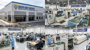
South Bay Circuits (SBC) has run design, fabrication, assembly, and box builds under one roof since 1981, which removes those handoff gaps entirely.
That single-source model matters most on boards where a missed clearance calculation or an unverified laminate substitution creates a genuine safety risk, well beyond the cost of rework. SBC's 60,000+ square foot Chandler, Arizona facility supports the full process without shipping boards between separate companies at each stage.
SBC's certifications line up with the industries that rely most heavily on HV design discipline:
- ISO 9001:2015: quality management across the full manufacturing process
- AS9100: aerospace-specific quality requirements
- ISO 13485 compliance: medical device manufacturing standards
- ISO/TS 16949 compliance: automotive quality requirements
- ITAR registration and CMMC Level 1 compliance: defense program requirements
Certifications establish the compliance baseline, but speed matters just as much when you're refining creepage-critical prototypes. SBC's quick-turn capabilities, including PCB fabrication in as fast as 24 hours and same-day assembly options, let engineering teams test spacing and material changes without losing weeks to a slow revision cycle.
If you're working through clearance calculations or material selection on a high-voltage board, SBC's team can talk through your stack-up and certification path before you commit to fabrication.
Frequently Asked Questions
What is a high-voltage PCB?
A high-voltage PCB is a board designed with the spacing and insulation needed to safely manage voltages that pose an arcing or shock risk. Compared to a standard board, it differs in clearance, creepage, material CTI rating, and often conformal coating.
How many volts can a PCB handle?
It depends entirely on the design. A standard FR4 board handles a few hundred volts safely under clean conditions, while a properly engineered high-voltage board with adequate spacing and coatings can manage several kilovolts.
What is the best material for a high-voltage PCB?
High-CTI laminates and higher resin content deliver the best performance at elevated voltages. Standard FR4 still works fine for lower HV ranges where budget matters more than margin.
Does high-voltage PCB design require different manufacturing processes?
Yes. Fabrication demands wider spacing and adjusted dielectric layouts, while assembly requires controlled conformal coating and tighter cleanliness standards. These extra steps affect both cost and lead time.
What is the difference between clearance and creepage?
Clearance is the shortest through-air distance between two conductors, while creepage is the shortest path along an insulating surface between them. Both require independent verification: clearance failures cause instant arcing, and creepage failures develop through gradual surface tracking.
What standards apply to high-voltage PCB design?
IPC-2221 governs generic spacing and clearance rules, IEC 60664-1 handles insulation coordination, and UL 796/UL 61010 cover safety certification for the board and end equipment. Most HV products need to satisfy more than one of these depending on their certification path.