Introduction
A medical imaging system pairs a high-speed signal processing board with a separate analog front end. A defense avionics unit uses a backplane with hot-swappable plug-in modules. In both cases, the product only works when every board connects correctly — electrically, mechanically, and logically. Most modern electronic products rely on exactly this kind of multi-board architecture.
That interdependency is what separates multi-board design from single-board work. A wiring error on one board stays invisible until both boards are assembled together, which is exactly when it's most expensive to fix. Nearly 60% of PCB designers report one to five respins annually, and inter-board connection errors are among the hardest to catch before bring-up.
This guide covers the complete multi-board workflow: system planning, electrical design for cross-board connectivity, mechanical integration, and manufacturing handoff, with practical guidance at each stage.
Key Takeaways
- Multi-board design requires system-level thinking before the first schematic line is drawn
- Each board should own one functional domain — power, I/O, signal processing — to simplify debugging
- Confirm ground continuity and connector pinout on both mating sides before layout begins
- Maintain separate BOMs and fabrication packages at both the board level and system level to prevent production errors
- Consolidating fabrication and assembly under one manufacturer simplifies cross-board compatibility checks and reduces handoff errors
What Is Multi-Board PCB Design and When Should You Use It?
Defining the Approach
A multi-board PCB design is a system-level architecture where two or more physically separate PCBs are electrically and mechanically interconnected to function as a complete product. This is distinct from a single large board (one PCB doing everything) or assembly variants (different stuffing configurations of the same board).
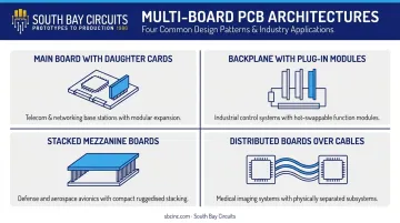
The four most common architectures:
- Main board with daughter cards — a central processor board with plug-in cards for specific I/O or RF functions; common in medical imaging devices where the analog front-end card is swapped by modality
- Backplane with plug-in modules — a passive or active bus board into which functional modules plug; the PXI Express standard uses this architecture across military, aerospace, and industrial automation, with controller-to-backplane bandwidth reaching 6 GB/s
- Stacked mezzanine boards — two parallel boards connected by high-density mezzanine connectors; PICMG's AdvancedMC standard defines this approach for customizable I/O in telecom and defense chassis
- Distributed boards over cables — boards separated by distance, connected via wire harnesses or FPC ribbons; common in automotive electronics and industrial enclosures
Why Split Across Multiple Boards?
Designers choose multi-board architectures for specific, practical reasons:
- Enclosure constraints — the product geometry simply doesn't fit a single large PCB
- Modularity — independent boards can be repaired or upgraded without replacing the entire assembly
- Functional isolation — separating analog and digital domains on distinct boards reduces noise coupling
- Independent sub-assembly testing — each board can be validated before system integration
- Revision cost management — when only one subsystem changes, only that board gets a new revision
Where Multi-Board Design Is Most Common
Aerospace, defense, medical devices, industrial instrumentation, and automotive electronics all rely heavily on multi-board architectures. These sectors also impose higher reliability and traceability standards on board interconnections — connector-level failures in a flight control system or an implantable device carry consequences that consumer electronics simply don't.
The core challenge is timing. An error in connector pinout or net assignment is invisible until boards are physically assembled together — at which point you're looking at rework, potential board scrapping, and schedule delays. Catching the same error during schematic review costs a fraction of that. Upfront planning is where multi-board projects are won or lost.
How to Plan Your Multi-Board PCB System
Step 1 — Define Board Functions First
Before drawing a schematic, assign each board a specific functional domain. Examples:
- Board A: power management and regulation
- Board B: digital signal processing
- Board C: analog I/O and sensing
- Board D: external communication interfaces
This prevents shared-component confusion, makes debugging faster, and clarifies ownership when one board needs a revision.
Step 2 — Determine Physical Arrangement
Resolve board orientation — stacked vertically, side-by-side, or right-angle at an enclosure wall — before layout begins. Bring a mechanical engineer in early.
The enclosure defines available volume and the assembly sequence constrains board order. A late-stage fit failure means an ECO that touches both mechanical and electrical deliverables simultaneously.
Step 3 — Choose Your Interconnect Method
| Interconnect Type | Best For | Key Trade-off |
|---|---|---|
| Board-to-board mezzanine connectors | Stacked parallel boards | Low profile, but fixed board-to-board spacing |
| Edge connectors | Backplane/plug-in module systems | High signal density, but constrains PCB edge routing |
| FPC/FFC ribbon cables | Angled or flexible connections | Permits arbitrary routing, requires strain relief and impedance management |
| Wire-to-board cables | Widely separated boards | Maximum flexibility, highest assembly labor |
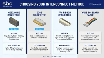
Molex mezzanine families support data rates up to 12.5 Gbps at 1.27 mm pitch; edge connector families reach 25 Gbps — product selection should be driven by actual signal speed requirements, not category maximums.
Step 4 — Map Signals Across Connectors Deliberately
This is where most logical errors enter the design. Best practices:
- Group related signals together on the connector (all SPI signals on adjacent pins, not scattered)
- Place ground pins adjacent to every high-speed signal pair — Samtec's signal integrity guidance notes that a 1:1 signal-to-ground ratio is typical for single-ended pin mapping
- Document the pinout on both the transmitting and receiving side of every connector before finalizing the schematic
- Verify that each connector symbol has the correct gender, orientation, and pin numbering reflected accurately in both child schematics
Step 5 — Keep Schematics Separate by Board
Maintain a distinct schematic set for each PCB. Never mix components from different boards on the same schematic sheet. Tools like Altium Designer represent each child PCB as a separate module in the system schematic, enabling cross-board connectivity validation before layout begins — and keeping revision control clean when one board updates independently.
Electrical Design: Connectivity, Ground, and Signal Integrity
Validating Cross-Board Connections Before Layout
Every net that crosses a board boundary must appear explicitly in the schematic on both sides — the sending connector and the receiving connector. When this step is skipped, the failures that follow during bring-up include:
- Rotated connectors that reverse an entire row of signals
- Transposed rows that swap adjacent signal groups
- Open nets where a signal is defined on one board but missing on the mating connector
- Short circuits where two nets accidentally share a pin assignment
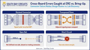
None of these failures are detectable during single-board design review. All are detectable during a focused cross-board ERC check before fabrication.
Ground Continuity Strategy
Each board should use a solid ground plane, and every board-to-board connector should include dedicated ground pins to tie the references together. This establishes two essentials:
- A consistent impedance reference for signals crossing board boundaries
- A controlled return path that prevents ground loops
For enclosed multi-board systems sharing a chassis, a common ground through the connector stack is usually sufficient. Boards in separate enclosures — or those with significant high-current power domains — face a different challenge: ground potential difference between boards becomes a direct reliability risk that requires deliberate management.
When to Use Differential Protocols
Single-ended signals are adequate for short, controlled inter-board connections within a shared enclosure. For longer cable runs, physically separated enclosures, or high-current DC systems where ground offsets are likely, switch to differential protocols:
- CAN bus — Analog Devices notes that CAN's wide common-mode range handles ground-potential differences between nodes, making it well-suited for distributed automotive and industrial systems
- RS-485 — TI's RS-485 design guide recommends assuming large ground-potential differences for remote links, with galvanic isolation as the reliable prevention method when required
- Ethernet — MDI traces should be routed as differential pairs with a continuous ground reference underneath
Protocol selection turns on four factors: the physical-layer standard, required ground-offset tolerance, EMI targets, and connector channel characteristics. When any one of those factors exceeds the capability of a single-ended link, a differential protocol is the right call.
Connector-Level Signal Integrity
For high-speed signals crossing board boundaries:
- Maintain controlled-impedance traces up to the connector body — do not let the trace geometry change within 10 mils of the connector pad
- The return path interrupts at the connector; ground pins placed adjacent to signal pins restore continuity and reduce crosstalk
- Impedance discontinuities at the connector interface generate reflections — connector selection should include a matched differential impedance target (TE's Fortis Zd connector specifies 100 ohm ±10% for high-speed applications)
- Minimize stubs and vias in the signal path at the connector entry point
Mechanical Integration and 3D Assembly Considerations
Why Mechanical Collaboration Is Non-Negotiable
The mechanical engineer's decisions — enclosure geometry, assembly sequence, cable routing, spatial conflicts — directly constrain PCB layout before a single trace is routed. Starting layout without that input means making assumptions that require expensive rework once the STEP files arrive.
Key constraints that must be locked in before layout begins:
- Maximum board height (component side and solder side) within the enclosure
- Assembly order — which board goes in first determines which connectors must be accessible during installation
- Cable routing paths and bend radius requirements for FPC connections
- Clearance zones for assembly tooling and fasteners
3D Interference Checking
Using STEP models for each board and its tallest components, the designer or MCAD engineer can verify:
- No board or component collides with another board, enclosure wall, or fastener
- Connector mating heights are correct: TE's floating connector families allow ±0.6 mm float for blind mating, but that tolerance must be confirmed against the actual assembly stack
- Clearance exists for cables and their strain relief features
- Assembly tooling can reach all fasteners and connectors in the assembly sequence
Catching fit failures here prevents ECOs that force simultaneous rework on both the PCB layout and the mechanical enclosure — a combination that consistently drives the highest change costs in multi-board programs.
Stacking and Interconnect Geometry Trade-offs
Each interconnect geometry resolves the fit-versus-routing trade-off differently — the right choice depends on enclosure envelope, signal requirements, and rework access:
- Vertical mezzanine stacking: saves X/Y footprint but adds Z height. Samtec flexible-stacking families span 1.65 to 48.51 mm board separation, so stack height is configurable — validate against the enclosure envelope before committing.
- Right-angle edge connectors: mate at the board edge for backplane applications, preserving Z height, but constrain signal routing near the edge and limit rework access.
- FPC ribbons: accommodate non-parallel board orientations and arbitrary routing angles, but require deliberate strain relief design and impedance control for high-speed signals.
Managing BOMs and Design Data for Multi-Board Projects
The Data Hierarchy
Multi-board manufacturing operates at two levels simultaneously:
- PCB level — fabrication files, pick-and-place data, assembly drawing, and BOM for each individual board
- System level — combined BOM for procurement visibility, shared-component tracking, and total cost calculation; system-level assembly drawing showing how all boards relate in the final product
Fabrication data is generated separately for each board and its panel. Pick-and-place data is strictly PCB-level. Collapsing these levels — for example, combining components from two boards into a single BOM — directly causes kitting errors in production.
BOM Management Best Practices
- Use a consistent part numbering system that ties each component back to its parent board
- Add a board/PCB column to the combined system BOM so procurement can identify parts shared across multiple boards
- Flag shared components explicitly — a component used on both Board A and Board B must appear in the combined BOM with quantities summed, not listed twice as separate line items
- Run a BOM scrub before releasing to production to catch obsolete or long-lead parts that could affect multiple boards simultaneously
Version Control and Change Tracking
Store each board's design files separately in a version-controlled repository and assign revision numbers at the individual board level. Cross-board dependencies need explicit tracking — not just documentation.
When a connector change on Board A requires a matching change on Board B's mating connector, treat it as a linked revision event:
- Update both boards' revision numbers simultaneously
- Document the dependency in the change record
- Release the matched revision set to fabrication and assembly together — never one board ahead of the other
Preparing Your Multi-Board Design for Fabrication and Assembly
What a Complete Manufacturing Package Includes
For each board, the fabrication package should contain:
- Gerber (RS-274X) or ODB++ fabrication files
- Drill files with tooling legend
- Pick-and-place files for every assembly side
- Assembly drawing with component orientation callouts
- PCB-level BOM with reference designators
In addition, the system-level package should include a system assembly drawing that shows how all boards fit together, connect, and orient relative to each other. Sending individual board packages without this system context is a common cause of connector orientation errors at the assembler — the assembler cannot know from a single-board drawing that a header on Board A must face left to mate with the receptacle on Board B.
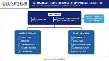
All packages must be clearly labeled with part numbers and revision levels. When multiple boards share the same connector part number, revision mismatches between boards produce assembly errors that are difficult to trace after the fact.
The Value of a Single-Source Manufacturer
When one partner handles fabrication and assembly for all boards in a multi-board system, that partner can cross-check connector compatibility across boards before production begins. With multiple vendors — each handling one board — no single party has visibility into the complete system. A reversed connector pinout on Board A only becomes apparent when that vendor's board is mated with another vendor's Board B, at which point both parties point to the other's documentation as the source of error.
South Bay Circuits (SBC) operates as a single-source contract manufacturer covering PCB design, fabrication, and assembly from its 60,000 sq ft facility in Chandler, AZ. For multi-board programs in aerospace, defense, medical, and industrial sectors — where connector-level errors carry regulatory consequences, not just rework — single-source accountability eliminates the cross-vendor blame problem entirely.
SBC's specific advantages for multi-board programs include:
- Process traceability: ISO 9001:2015 certification and over 40 years of manufacturing experience back every build
- Speed: 24-hour bare board fabrication and 3-Day Turn or Less assembly compress the prototype-to-validation cycle
- Reduced iterations: Complete in-house visibility means connector compatibility issues are caught before production, not after
Frequently Asked Questions
What is the difference between a multi-board design and a single PCB with variants?
A multi-board design involves physically separate PCBs that are electrically connected and assembled together as a working system. Design variants are different stuffing configurations of the same physical board. Both techniques can coexist — a multi-board system might use assembly variants on one of its boards.
When should you use a multi-board design instead of a single larger PCB?
When the product geometry won't fit one board, when modular repairability is required, when analog and digital domains must be physically isolated, or when the enclosure form factor forces the design to split across separate physical assemblies.
What connector types are commonly used to connect multiple PCBs?
Common options include:
- Board-to-board mezzanine connectors
- Pin headers and edge connectors
- FPC/FFC ribbon connectors
- Wire-to-board cable assemblies
The best choice depends on board orientation, signal speed requirements, and available space in the enclosure.
How do you maintain signal integrity across board-to-board connections?
Maintain controlled-impedance traces up to the connector and place ground pins adjacent to high-speed signals for a clear return path. For long or electrically noisy inter-board links, use differential protocols such as RS-485, CAN, or Ethernet where a shared ground reference cannot be guaranteed.
What are the most common errors in multi-board PCB design?
Rotated or mirrored connector orientation producing a reversed pinout, missing ground pins at the board interface causing a floating reference, and net assignment mismatches (opens or shorts) that only surface during board bring-up. All three are preventable through cross-board ERC validation before fabrication.
How should fabrication files be organized for a multi-board project?
Each board requires its own complete package (Gerbers, drill files, BOM, and assembly drawing) labeled with part number and revision level. Include a system-level assembly drawing showing all boards in context to prevent orientation errors at the assembler.