Introduction
A pacemaker, an aerospace flight controller, a car's anti-lock braking module — all of them depend on a circuit board that was assembled correctly the first time.
One missed solder joint or mismatched component can delay a product launch by weeks or trigger a field failure that costs far more to fix after shipment.
Adding to the confusion: many engineers and buyers use "PCB" when they actually mean "PCBA," and that mix-up creates real problems when requesting quotes or comparing manufacturers.
This guide breaks down what PCB assembly actually involves and how the process works step by step. You'll also learn what separates reliable production from risky production, what drives cost, and how to pick a manufacturing partner you can trust.
Key Takeaways
- A PCB is the bare board; a PCBA is that same board once components are soldered on and functioning
- Most assemblies combine SMT and PTH techniques depending on component types
- Testing methods like AOI, ICT, and X-ray each catch different defect categories, but none catches everything alone
- Component pricing, not board size, usually drives the biggest share of assembly cost
- Single-source manufacturers cut handoff risk between fabrication and assembly
What Is Printed Circuit Board Assembly (PCBA)?
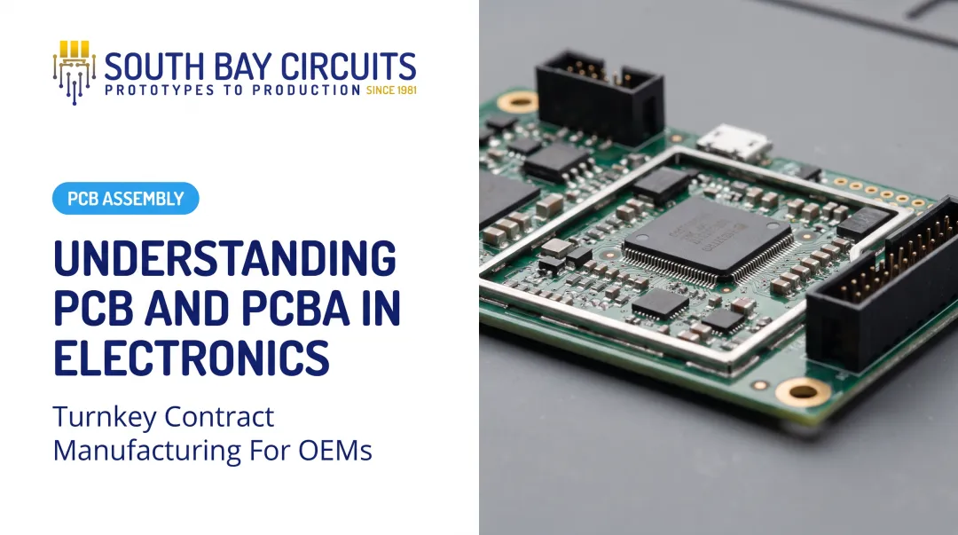
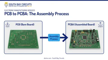
A PCB is the unpopulated, laminated substrate — copper traces etched into fiberglass, providing the electrical pathways and physical structure a device needs. On its own, it does nothing. There's no functionality until components go on.
A PCBA (also called PCA or CCA, depending on who you ask) is that same board after every resistor, capacitor, connector, and integrated circuit has been mounted and soldered into place. According to IPC's guidance for printed board assemblies, fabrication and assembly are treated as distinct manufacturing stages, with the board itself as the input and the populated assembly as the output.
PCBA vs. PCB: Key Differences
A PCB is the raw board — nothing more than copper and fiberglass. The PCBA is that same board fully populated and ready to function inside a device.
- PCB fabrication comes first: etching, drilling, plating, and lamination create the bare board
- PCB assembly follows as a separate stage: components get placed and soldered onto that board
- Only the PCBA is a working electronic circuit ready for integration into a device
Why the Distinction Matters for Sourcing
Mixing these terms up when requesting a quote causes real friction. Manufacturers need to know whether you're asking for bare boards, populated assemblies, or both, because the documentation, lead time, and pricing vary widely between the two.
Before assembly can start, you'll typically need:
- A complete Bill of Materials (BOM)
- An Approved Vendor List (AVL) for component sourcing
- Gerber files for the board layout
- A centroid or pick-and-place file for component positioning
Manufacturers like South Bay Circuits (SBC) manage both fabrication and assembly under one roof at their Chandler, Arizona facility. That setup removes the queue and shipping time that stacks up when a bare board has to travel from one vendor to a completely separate assembly shop.
The PCB Assembly Process: From Bare Board to Finished Product
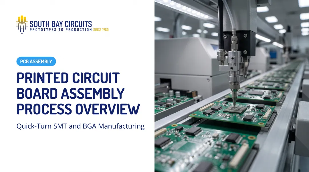
At a high level, PCB assembly moves through a consistent sequence: solder paste goes down, components get placed, everything gets soldered, then inspected and tested before it ships. The specific techniques used depend heavily on the components involved.
Surface-Mount Technology (SMT) vs. Through-Hole (PTH) Assembly
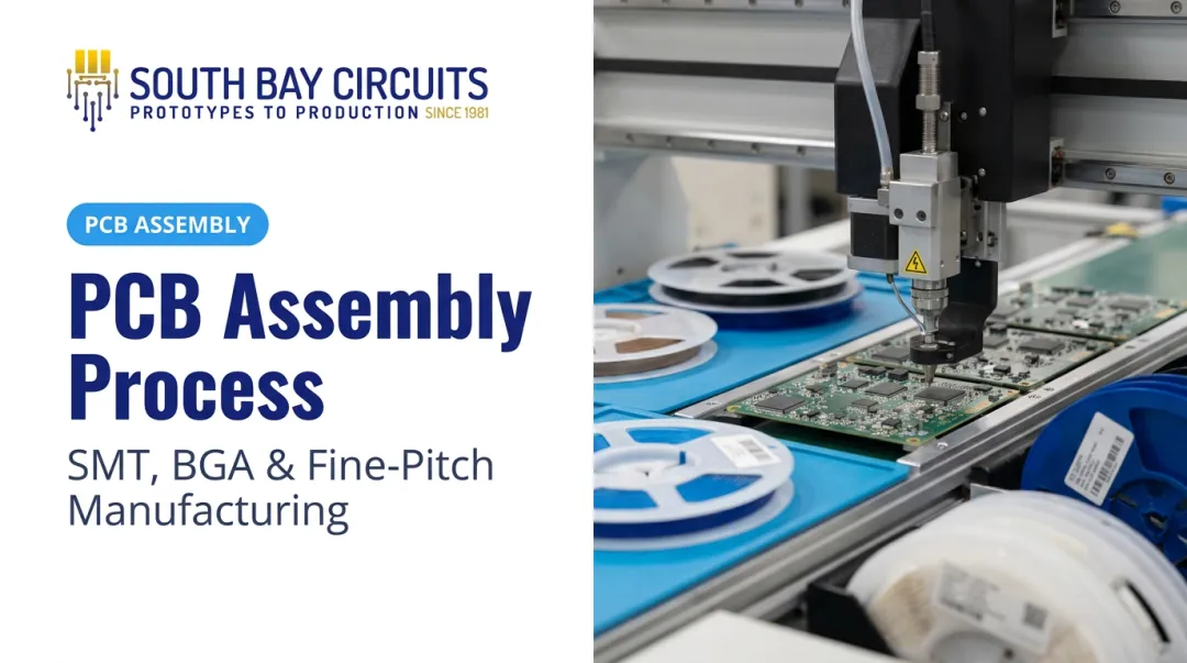
SMT places components directly onto pads on the board surface, then reflow-solders them in a controlled oven. It's the go-to method for compact, high-volume, automated production runs where component density matters.
PTH (also called through-hole assembly) inserts component leads through drilled holes, then solders them using wave or selective soldering. It's the preferred choice for parts that need mechanical strength, such as connectors, transformers, and high-power components that take physical stress during the product's life.
Per an IPC technical paper on mixed-technology assembly, SMT has been the dominant approach since the early 1990s largely due to density and cost advantages, while through-hole has held its ground specifically for connector joints that need mechanical robustness.
Most real-world boards need both. A single assembly might carry SMT resistors and ICs alongside PTH connectors, so the manufacturing line needs to support mixed-technology processes like selective wave soldering or pin-in-paste (intrusive reflow). In pin-in-paste, extra solder paste is printed at the through-holes so those joints form during the same reflow cycle as the SMT components.
Step-by-Step PCB Assembly Workflow
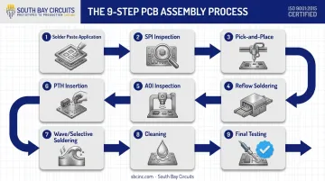
Here's the typical sequence for a mixed-technology board:
- Solder paste application — paste is printed onto SMT pads through a stencil
- Solder paste inspection (SPI) — verifies paste volume and placement accuracy
- Pick-and-place — automated equipment positions SMT components onto the pasted pads
- Reflow soldering — the board passes through a reflow oven, melting the paste to form permanent joints
- Automated optical inspection (AOI) — checks placement and solder joint quality
- PTH insertion — through-hole components get inserted, manually or via automated insertion
- Wave or selective soldering — solders the through-hole joints
- Cleaning — removes flux residue and contaminants
- Final testing — confirms the assembly performs as designed
None of this can start without a finalized documentation package. A missing BOM line item or an outdated fabrication drawing is one of the most common reasons quotes stall or assembly runs get delayed.
At SBC, incomplete documentation causes a large share of prototype order holdups. A standardized checklist covering design files, BOM, layout files, and fabrication drawings before submission catches these gaps before they cost you time.
Ensuring Quality: Testing and Inspection in PCB Assembly
Assembly isn't finished when the last component gets soldered. Testing is what separates a production run you can trust from one that generates warranty returns.
Four inspection methods do most of the heavy lifting:
- AOI (Automated Optical Inspection): Camera systems scan for placement errors and visible solder defects
- ICT (In-Circuit Testing): Verifies electrical connectivity and component values against the design
- X-ray inspection: Reveals hidden solder joints underneath components like BGAs, where visual inspection can't reach
- Functional testing: Confirms the board actually performs its intended job under real operating conditions
No single method catches everything. A study referenced in IPC's technical resources on universal test strategy tested these methods against 100 known defects. AOI detected 59%, X-ray/AXI detected 91%, and ICT detected 52% — proof that layered testing, not any single method, protects reliability.
That's exactly why manufacturers serving strict-reliability industries stack multiple test methods and hold certifications tied to those sectors:
| Industry | Relevant Certification |
|---|---|
| Medical devices | ISO 13485 |
| Aerospace/defense | AS9100 |
| Automotive | ISO/TS 16949 |
SBC maintains ISO 9001:2015 certification along with ISO 13485, AS9100, and ISO TS 16949 compliance across its Chandler facility. This supports customers in medical, aerospace, automotive, and defense programs where documented quality processes aren't optional.
How Much Does PCB Assembly Cost?
PCB assembly pricing isn't just about board dimensions. Several factors combine to determine your final unit cost.
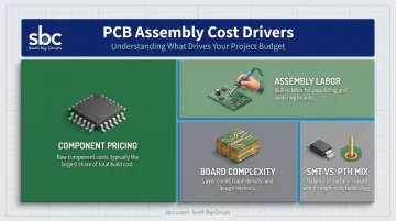
Primary cost drivers:
- Component pricing — usually the largest single cost category, especially for boards with expensive ICs or specialty parts
- Assembly labor — driven by placement count, technology mix, and handling complexity
- Board complexity — layer count, trace density, and fine-pitch requirements all add process steps
- SMT vs. PTH mix — SMT dominates most unit counts and carries lower labor cost per placement, while PTH parts need manual or semi-automated handling that adds cost per part
Volume matters too. Prototype and low-volume runs carry a per-unit cost premium compared to standard production.
That premium comes from non-recurring engineering (NRE) costs like pick-and-place programming, stencils, reflow setup, and test fixture development. These costs get spread across fewer units, so a run of 25 boards absorbs NRE very differently than a run of 5,000.
Exact percentage savings vary too much by design and component mix to quote a universal number. Instead, request a quote that separates recurring costs (BOM, placement, test) from one-time NRE. That breakdown shows exactly where your money goes and where volume will actually help.
Choosing the Right PCB Assembly Partner
Not every assembly house is equipped for every job. Before committing, buyers should evaluate a few specific things.
Certifications relevant to your industry:
- ISO 9001 for general quality management
- ITAR registration if you're working on defense-related hardware
- ISO 13485, AS9100, or IATF 16949 depending on your target market
Capability and process control:
- In-house fabrication plus assembly (versus outsourced steps)
- Documented turnaround times for both prototype and production runs
- Fine-pitch and BGA placement capability if your design requires it
Why single-source matters:
When fabrication and assembly happen at separate companies, every miscommunication becomes a finger-pointing exercise. Who's responsible when a board fails testing: the fab house that etched it, or the assembler that populated it?
SBC eliminates that ambiguity by handling PCB design, fabrication, and assembly under one 60,000+ square foot roof in Chandler, Arizona, with decades of experience across medical, aerospace, automotive, and industrial programs.
One more thing worth asking about upfront: design-for-manufacturing (DFM) feedback. A manufacturer that reviews your layout before production starts (flagging fine-pitch concerns, footprint issues, or unusual component orientations) saves you from discovering those problems mid-run, when a redesign costs real time and money.
Frequently Asked Questions
What is a printed circuit assembly?
A printed circuit assembly (PCA) is a printed circuit board that's been fully populated with soldered electronic components. It's the functional version of the board, ready to operate inside a finished device.
What's the difference between a printed circuit assembly (PCA) and a printed circuit board (PCB)?
A PCB is the bare, unpopulated board — just copper traces on a substrate. A PCA is that same board after components have been assembled and soldered onto it, making it functional.
How much does printed circuit assembly cost?
Cost varies widely based on component pricing, board complexity, and production volume. The most accurate way to estimate cost is requesting a detailed quote from a manufacturer based on your specific BOM and design files.
What is the difference between PCB and PWB?
PWB (printed wiring board) traditionally refers to the bare board without components, similar to how PCB is used today. "PCB" is now the more common term, though PWB still appears in some military and legacy specifications.
How long does PCB assembly typically take?
Turnaround depends on design complexity, component availability, and order volume. Single-source manufacturers handling both fabrication and assembly typically compress timelines compared to coordinating separate vendors.
What certifications should a PCB assembly manufacturer have?
Look for ISO 9001 as a baseline, plus industry-specific credentials like AS9100 (aerospace), ISO 13485 (medical), or ITAR registration (defense) for your market. These certifications signal documented quality and compliance processes, not marketing claims.