PCB design services typically include:
- Schematic capture and circuit design
- Layout and routing
- Design rule checking (DRC)
- Gerber file generation for manufacturing
This guide breaks down what actually drives PCB design costs, what you should expect to pay at each complexity level, which hidden costs catch buyers off guard, and how to keep your total project budget realistic from the start.
Key Takeaways
- Design fees typically run $500–$10,000+ and rarely include fabrication or assembly
- Layer count, materials, and designer expertise drive most of your quote
- Hidden costs (prototypes, tooling, compliance, hand-offs) often exceed the design quote
- Complete schematics, BOM, and mechanical constraints upfront prevent costly change orders
- One provider for design through assembly cuts coordination cost and cycle time
Key Factors That Influence PCB Design Costs
PCB pricing isn't arbitrary. It comes down to four variables: how complex the board is, what it's made of, who's designing it, and how fast you need it.
Design Complexity and Layer Count
Layer count is the single biggest driver of engineering hours. A board with one connector and a handful of components might take a designer just 5 to 6 hours. A dense, constraint-heavy multilayer board built to fit inside a tight enclosure can require 360+ hours of layout work, according to engineering marketplace Cad Crowd's PCB design pricing research.
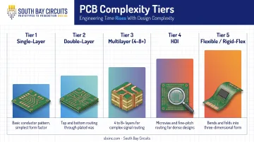
Rough complexity tiers, from least to most engineering time:
- Single-layer — basic circuits, minimal routing
- Double-layer — moderate component density, still straightforward
- Multilayer (4-8+ layers) — signal integrity, power planes, and impedance control add real time
- HDI (High-Density Interconnect) — blind/buried microvias and tight buildup rules add substantial layout time
- Flexible/rigid-flex — mechanical constraints and bend zones add another layer of review
Materials and Specifications
Most boards use standard FR-4 because it balances thermal performance, dimensional stability, and cost. But FR-4 isn't always the right call.
- Rogers laminates (RO4000 series) — used in RF, satellite, cellular, and radar applications where loss needs to stay low
- Polyimide — rated for high-temperature military, commercial, and industrial use
- Ceramic (Al2O3) — common in power modules, EV power electronics, and 5G/high-frequency circuits
- Aluminum-clad — built for heat dissipation in LED lighting, power converters, and automotive electronics
Specialty materials raise both material cost and design time, since routing and thermal management change with each substrate. South Bay Circuits' design team regularly works with Rogers and polyimide substrates on multilayer and high-frequency boards where those tradeoffs matter.
Designer Expertise and Geographic Location
Hourly rates vary widely depending on who you hire:
| Experience Level | Typical Rate |
|---|---|
| Entry-level | $25 – $75/hour |
| Mid-level | $75 – $150/hour |
| Expert/senior | $150 – $300+/hour |
Most professional PCB designers charge $95 to $145 an hour, with specialists commanding up to $300 an hour, per Cad Crowd's rate benchmarking.
Freelancers tend to run cheaper than design firms, but a lower hourly rate isn't automatically a lower total cost. A freelancer quoting fewer dollars per hour can still land at a higher project total if they need more hours than an experienced firm would.
South Bay Circuits' design work is based onshore in Chandler, Arizona, with remote design collaboration available nationwide — no offshore design handoffs to manage.
Turnaround Time and Add-On Services
Rush timelines cost money. Compressing a standard multi-day schedule into a same-day or 24-hour turnaround typically carries a premium, since it means bumping other jobs in the queue.
Add-on services also build on top of the base design fee:
- DFM (Design for Manufacturability) review — checks for issues before fabrication
- Simulation or signal-integrity testing — usually quoted per project, not standard-priced
- Prototyping — often billed separately from the design fee itself
South Bay Circuits folds DFM and DFT (Design for Testability) review into its standard design process rather than treating them as bolt-on charges.
How Much Does PCB Design Cost? Typical Price Ranges
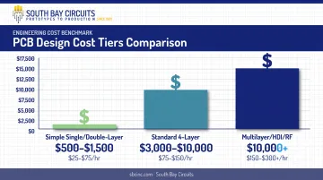
Here's where the numbers actually land. According to pricing benchmarks published by PCB service provider WonderfulPCB, a small board using standard components typically costs $500 to $1,500 to design.
A typical 4-layer board runs $3,000 to $10,000. High-density or RF designs can exceed that range entirely.
| Complexity Level | Typical Design Cost | Example Hourly Range |
|---|---|---|
| Simple single/double-layer | $500 – $1,500 | $25 – $75/hour |
| Standard 4-layer | $3,000 – $10,000 | $75 – $150/hour |
| Multilayer / HDI / RF | $10,000+ | $150 – $300+/hour |
Important distinction: these figures cover design only: schematic, layout, routing, DRC, and Gerber output. They don't include fabrication or assembly.
- Design cost = engineering time to create and verify the layout
- Fabrication/unit cost = materials, layer count, copper weight, and production volume
Turnkey quotes often bundle both into one number, which makes it hard to know what you're actually paying for. Ask for the two line items separately.
Decisions made during design—layer count, trace width, material choice—directly shape fabrication and assembly costs later. Treat design and manufacturing as one linked decision, not two separate handoffs.
Hidden Costs in PCB Manufacturing You Should Watch For
The quoted design fee is rarely the final number. Here's what tends to show up later:
- Prototyping and iteration costs. Most projects need several prototype rounds; each adds material, tooling, and engineering time—often up to about $2,000 per iteration.
- NPI and tooling/setup fees. New Product Introduction charges cover one-time engineering and tooling that often isn't itemized up front. On volume runs, tooling, stencil, and test fees are usually paid once.
- Certification and compliance testing. UL, FCC, CE, ISO 13485 (medical), and AS9100 (aerospace) testing sits outside base design and fab pricing and can add major line items.
- Vendor hand-off and coordination costs. Splitting design, fab, and assembly across vendors adds inter-stage shipping, queue time, and rework when specs don't align.
- Shipping, logistics, and delay costs. Offshore sourcing can add freight, customs, and time-zone delays that rarely appear on the initial quote.
How to Reduce PCB Design and Manufacturing Costs
Cost control mostly comes down to preparation. Three steps make the biggest difference:
- Define requirements clearly upfront. Complete schematics, a verified BOM, and mechanical constraints cut revisions, and every revision adds engineering hours. Incomplete documentation causes questions or issues on nearly half of all prototype orders, according to South Bay Circuits' internal quoting data.
- Simplify where it doesn't hurt performance. Standard layer counts, common materials, and typical trace widths avoid manufacturing surcharges and speed up production.
- Match the provider to the project. A low-cost freelancer can work for a simple board. Regulated or complex work (medical, aerospace, automotive) needs an experienced, quality-certified provider.
Design decisions carry more financial weight than most buyers assume. Roughly 70% of total product manufacturing cost gets locked in during the design cycle, according to I-Connect007's Design007 reporting on PCB cost drivers. Getting the design right the first time is the biggest cost lever you have.
Why a Single-Source PCB Partner Reduces Total Project Cost
Splitting design, fabrication, and assembly across multiple vendors sounds cheaper on paper. In practice, it multiplies hidden costs: shipping between each stage, inconsistent quality standards from vendor to vendor, and finger-pointing when a defect shows up and nobody wants to own it.
South Bay Circuits (SBC) runs the opposite model. Founded in 1981, SBC operates from a 60,000-square-foot facility in Chandler, Arizona. The company handles design, fabrication, and assembly under one roof, with fabrication in as little as 24 hours and same-day assembly available.
What that consolidation actually gets you:
- ISO 9001:2015, AS 9100, and ISO 13485 compliance, plus ITAR registration and CMMC Level 1 status
- One engineering team evaluating manufacturability and cost from the first design review through final test
- No inter-company shipping or queue time between design, fab, and assembly stages
- One point of accountability if something needs to be fixed
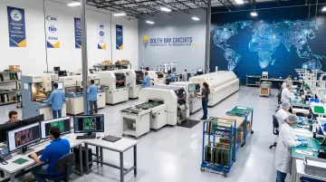
For buyers in aerospace, defense, medical, automotive, and industrial sectors, a single certification gap or spec mismatch can stall a program. Single-source structure turns that risk into more predictable project costs and faster cycle time.
Frequently Asked Questions
How much does a PCB cost?
Design costs alone typically range from about $500 for a simple board to $10,000+ for complex or high-frequency designs. Total project cost, including fabrication and assembly, depends on volume and board specifications.
What are the hidden costs in PCB manufacturing?
Common hidden costs include multiple prototype iterations, NPI and tooling fees, certification and compliance testing, and vendor coordination or shipping costs between separate design, fab, and assembly providers.
What's typically included in a PCB design service?
Core deliverables include schematic design, layout and routing, design rule checking (DRC), and Gerber file generation for manufacturing.
Is it cheaper to design a PCB in-house or outsource it?
In-house design suits companies with dedicated engineering staff and steady project volume. Outsourcing to a specialist often reduces error-driven rework costs for one-off or highly complex projects.
How can I get an accurate PCB design cost quote?
Provide complete schematics, a detailed BOM, and mechanical constraints upfront. This helps providers quote accurately and avoids costly change orders once work has already started.
What's the difference between PCB design cost and PCB fabrication cost?
Design cost covers the engineering time needed to create the layout. Fabrication cost covers materials, layers, and manufacturing the physical board. Both are separate but connected line items in a turnkey project.