That unpredictability is exactly why RF PCB design is its own discipline. Engineers building wireless modules, radar systems, IoT sensors, and 5G hardware routinely run into three recurring headaches: signal loss, impedance mismatch, and EMI that can quietly degrade — or completely tank — a circuit's performance.
This guide breaks down the core layout principles that actually prevent those failures: stack-up strategy, the 3W rule, material selection, and the most common mistakes engineers make before a board ever reaches fabrication. We'll also cover why the manufacturer you choose matters just as much as the layout itself.
Key Takeaways
- RF traces above 1 GHz must be treated as transmission lines
- 50-ohm controlled impedance prevents signal reflection and power loss
- The 3W rule cuts crosstalk by spacing traces 3x trace width apart
- Standard FR-4 loses too much signal energy above 1 GHz
- Manufacturing precision determines if your RF layout survives fabrication
What Is RF PCB Design and Why Does It Matter?
RF PCB design is the process of engineering boards to reliably carry radio frequency signals, roughly defined by the FCC as 3 kHz to 300 GHz. Most real-world applications, though, cluster in a narrower band. Wi-Fi, Bluetooth, GPS, 5G, and automotive radar systems typically operate somewhere between 300 MHz and 6 GHz or higher.
These boards form the backbone of wireless communication modules, IoT sensors, automotive radar arrays, and satellite systems. Get the layout wrong: dropped connections, failed certifications, or a device that simply doesn't work as intended.
Key Differences Between RF and Standard PCB Design
At RF frequencies, a trace stops behaving like a simple wire and starts behaving like a transmission line. That means engineers need to control characteristic impedance (commonly 50 ohms) rather than just worrying about connectivity between two points.
There's also the skin effect to account for. Current at high frequencies travels along the outer surface of a conductor instead of through its entire cross-section. This means making a trace wider doesn't automatically improve performance, despite being a common assumption for engineers coming from digital design backgrounds.
Common Challenges in RF PCB Design
Three problems show up again and again in RF layouts:
- Impedance mismatch — Mismatched trace impedance produces an SWR above 1:1, causing power loss and weaker signal transmission
- EMI and noise sensitivity — RF circuits pick up interference easily, making shielding and physical isolation non-negotiable
- Material limitations — Standard FR-4 can't handle frequencies above roughly 1 GHz, pushing designers toward RF-grade laminates
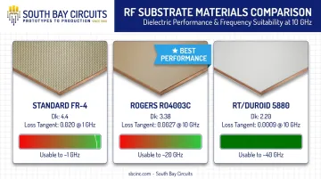
For that last point, the difference is measurable. Rogers RO4003C laminate runs a dielectric constant of 3.38 with a loss factor of just 0.0027 at 10 GHz, while PTFE-based materials like RT/duroid 5880 drop the dielectric constant even further, to around 2.2. Standard FR-4 simply can't compete at those frequencies.
Essential RF PCB Layout Principles
This is where theory becomes practice. Stack-up structure, trace routing, impedance control, and via placement determine whether your RF design performs as simulated or falls apart during testing.
Stack-Up Design for RF Boards
RF traces and components should sit on the top layer, backed immediately by a continuous ground plane, followed by a power plane. This is the standard convention for a 4-layer RF board.
| Layer Count | Best For | Trade-off |
|---|---|---|
| 2-layer | Rarely used for RF | Insufficient clearance, poor return paths |
| 4-layer | Simple RF designs | Good baseline, limited routing density |
| 6-12 layer | Complex, multi-signal RF designs | More routing flexibility, higher cost |
Keep the stack-up symmetric wherever possible. Symmetry promotes thermal stability and helps prevent the board from warping during reflow or thermal cycling, a detail that matters more on RF boards than most engineers expect.
Trace Routing and the 3W Rule
Here's a question that comes up in nearly every RF layout review: how far apart should parallel traces be? The answer is the 3W rule: keep the center-to-center spacing between parallel traces at least three times the trace width.
Testing documented in EDN found that increasing spacing from 1W to 3W reduced far-end crosstalk by 65% — a substantial improvement for a change that costs nothing in materials.
A few more routing habits worth building in:
- Keep RF trace lengths as short as possible to minimize attenuation
- Use 45-degree bends or mitered corners instead of sharp right angles
- Avoid unnecessary stubs and layer transitions along the signal path
Impedance Matching and Grounding
Characteristic impedance depends on three things: substrate thickness, trace width, and clearance from the ground plane. Get any of those wrong, and you'll see reduced power transfer and a worse signal-to-noise ratio.
Before you finalize any layout, run the trace geometry through an impedance calculator or simulation tool to confirm it hits your target impedance. Skipping this step is one of the most common (and most expensive) mistakes in RF design.
Equally important: maintain a continuous, unbroken ground plane directly beneath RF traces. Gaps in the ground plane create unintended loops that behave like accidental antennas, introducing noise you didn't design for.
Via Design and Shielding Considerations
Every via along an RF signal path adds parasitic inductance. Minimize their use, and when a layer transition is unavoidable, place ground vias close to the signal via to maintain a clean return path.
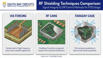
For isolating sensitive RF sections from digital or high-power circuitry, three shielding techniques do most of the heavy lifting:
- Via fencing: rows of ground vias that box in a signal path
- RF cans: physical metal shields soldered directly to the board
- Faraday cages: enclosures that block external field penetration
Material Selection for RF PCB Success
Standard FR-4 causes excessive signal attenuation once you push past 1 GHz, which is why most RF designers turn to PTFE-based or Rogers-style laminates instead. These materials hold a lower, more stable dielectric constant and loss tangent across a wider frequency range.
Copper foil quality affects RF performance too. Surface roughness on the copper affects signal loss at high frequencies. Rougher foil increases insertion loss, especially as frequency climbs and skin depth shrinks toward the scale of the roughness itself. Smoother foils are the better choice for RF applications.
For high-power RF designs, thermal conductivity and dimensional stability of the substrate become just as important as the electrical properties:
- Substrates need to resist dielectric property shifts under sustained heat
- Dimensional stability prevents impedance drift across temperature swings
- Copper-matched thermal expansion reduces stress on multilayer constructions
South Bay Circuits' RF/microwave engineers help customers select substrate stack-ups based on frequency, power, and layer-count needs.
Common RF PCB Design Mistakes and How to Avoid Them
Most RF board failures trace back to a few repeat offenders:
- Skipping trace width calculations for target impedance leads directly to signal reflection. Always verify trace geometry with a calculator or simulation tool before finalizing the layout.
- Poor grounding practices create noisy, unpredictable return paths when split ground planes and insufficient via stitching interrupt the current path. Fix it by maintaining one continuous, well-connected ground plane beneath every RF trace.
- Placing RF components too close to noisy digital or power circuitry invites interference that bleeds across short distances fast. Physical separation, dedicated RF zones, or shielding solves this before it becomes a debugging nightmare.
None of these mistakes are exotic; they're layout habits carried over from digital design that simply don't hold up at RF frequencies.
Why Partner with an Experienced RF PCB Manufacturer Like South Bay Circuits
A well-simulated RF layout still needs to survive fabrication without drifting from spec. Trace geometry, dielectric thickness, and via structures all have to be reproduced with tight tolerances, or the impedance calculations you ran during design won't hold up on the finished board.
South Bay Circuits has been fabricating and assembling PCBs since 1981, giving its team over four decades of experience translating layouts into physical boards that perform as designed.
What sets SBC apart operationally is its single-source model:
- Design, fabrication, and assembly all happen under one roof at its 60,000+ sq ft Chandler, Arizona facility
- This structure shortens NPI (new product introduction) timelines by removing the handoffs between separate vendors
- It also eliminates the "blame game" that often crops up during iterative RF prototyping, when multiple suppliers each point fingers at the others
SBC holds ISO 9001:2015 certification and maintains compliance with AS9100 (aerospace), ISO 13485 (medical), and ITAR requirements. For RF boards headed into defense, medical, or automotive radar applications, that certification stack provides the traceability and quality documentation those industries require before a board can ship.

Frequently Asked Questions
What is RF in PCB design?
RF stands for radio frequency, covering signals roughly from 3 kHz to 300 GHz. RF PCB design involves engineering boards that carry these high-frequency signals reliably, without excessive signal loss or interference.
What is the 3W rule in PCB?
The 3W rule states that center-to-center spacing between parallel traces should be at least three times the trace width. This minimizes electromagnetic coupling and crosstalk between adjacent signal paths.
What is the difference between RF PCB design and standard PCB design?
RF design treats traces as transmission lines requiring controlled impedance and specialized low-loss materials. Standard digital PCBs have more forgiving timing margins and rarely need this level of impedance control.
What materials are best for RF PCB design?
PTFE-based laminates and Rogers materials, such as RO4003C or RT/duroid series, are preferred for their low dielectric constant and loss tangent compared to standard FR-4. These properties keep signal loss manageable above 1 GHz.
How many layers should an RF PCB have?
Four-layer stack-ups are common for simpler RF designs, providing a signal layer, ground plane, power plane, and auxiliary layer. Complex designs with denser routing needs often move to 6-12 layers.
What is impedance matching in RF PCB design?
Impedance matching ensures the source, transmission line, and load all share the same characteristic impedance, often 50 ohms. This maximizes power transfer and minimizes signal reflection along the trace.