Introduction
A single misplaced 0402 resistor. One wrong reflow profile. That's often all it takes to turn a promising PCB design into an expensive respin — and a blown launch date.
Assembly errors are a common culprit behind delayed electronics launches. Yet many teams treat PCB assembly (properly called PCBA, or printed circuit board assembly) as an afterthought, something you hand off once the design files are done.
PCBA actually covers a lot of ground: solder paste application, component placement, reflow soldering, inspection, and final testing. Every stage carries its own failure points, and a mistake in any single one can compromise the entire board.
This guide breaks down the assembly process and shares practical, engineer-tested tips for design, sourcing, soldering, and inspection. The advice draws on decades of hands-on contract manufacturing experience, including that of South Bay Circuits (SBC), a single-source PCB design and assembly provider operating out of Chandler, Arizona since 1981.
Key Takeaways
- A single error at any stage can compromise the entire PCB assembly
- Design-for-Assembly (DFA) reviews before production catch most costly mistakes early
- Verified component sourcing and correct stencil selection directly affect defect rates
- AOI, X-ray, and flying probe testing catch solder defects invisible to the eye
- Single-source manufacturers reduce handoff errors and shorten overall cycle time
How PCBs Are Assembled: A Quick Process Primer
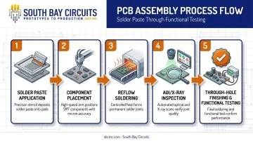
A bare PCB is just the substrate — copper traces, pads, and drilled holes with nothing mounted on it. Soldering components onto that substrate transforms it into a PCBA, a populated, functional board. Here's how that transformation happens.
Solder Paste Application & Component Placement
A stencil cut to match the board's pad layout applies solder paste to each pad. Paste thickness directly determines joint quality: too much risks bridging, while too little leaves joints weak or incomplete.
Pick-and-place machines then position surface-mount (SMT) components at high speed, often placing thousands of parts per hour with tight positional accuracy. Manufacturers insert through-hole parts manually or with automated equipment instead, depending on component size and board complexity.
Reflow Soldering, Inspection & Through-Hole Finishing
After placement, the board passes through a reflow oven that melts the solder paste and forms permanent electrical and mechanical joints. From there, boards typically move to Automated Optical Inspection (AOI) or X-ray inspection to catch misalignments, solder bridging, or missing components before they become bigger problems downstream.
Manufacturers then wave solder or selectively solder any through-hole components, depending on the mix of parts on the board. After soldering, boards undergo final electrical and functional testing to confirm they perform as designed before they ever ship.
Design-for-Assembly (DFA) Tips to Get It Right the First Time
DFA review happens before a single board hits the line. It's where incorrect footprints, tight part spacing, and drill file mismatches get caught. These are the kind of errors that otherwise trigger full respins weeks later.
IPC actively promotes DFM, DFT, and DFA as distinct, necessary practices in production preparation, and for good reason: catching a footprint mismatch on a review call costs a few minutes. Catching it after a failed reflow run costs a full production cycle.
A few tips that consistently prevent headaches:
- Provide a clean, accurate BOM with clear reference designators, orientation markings, and polarity indicators to prevent placement errors before they happen
- Include fiducial markers on the board so automated equipment and stencils can align accurately during paste application and placement
- Follow your assembler's published design rules for trace width, clearance, and drill sizes so the board manufactures cleanly without rework
- Flag non-washable, heat-sensitive, or hand-solder-only components clearly in your assembly notes so they get handled correctly, not run through a standard reflow cycle
At SBC, this is exactly why design and assembly sit under one roof. When the same engineers reviewing your layout also run the assembly line, a footprint or clearance issue gets flagged in the DFA review, not discovered on a failed board three weeks later.
Component Sourcing & Selection Tips
Sourcing decisions made months before assembly directly affect your defect rate.
ERAI recorded 1,055 suspect counterfeit and nonconforming parts in 2024 — the highest total since 2015, up 25% year-over-year, with analog ICs the most frequently reported part type (ERAI, 2024 Annual Report).
A few sourcing habits reduce that risk substantially:
- Buy from authorized distributors or verified suppliers. The Semiconductor Industry Association notes that counterfeit risk drops significantly when purchases go through original manufacturers and their authorized channels
- Choose integrated packages where possible. Combining multiple functions into one component reduces part count, board real estate, and overall cost
- Order a few spares beyond your build quantity. Extra components and boards give you room for rework, testing, or a mistake without triggering a whole new procurement cycle
Beyond following these habits, closing the sourcing gap means building component checks into the design phase itself. SBC references tools like ECIA Authorized during procurement planning, and treats component availability as a factor to resolve during design, not after boards are already fabricated.
Ordering materials before or alongside bare board fabrication keeps assembly moving the moment boards come off the line, instead of sitting in queue waiting on parts.
Soldering, Placement & Inspection Best Practices
This is where design intent meets physical reality. Get these details wrong and even a well-designed board can fail.
Match your stencil to your smallest components. Stencil thickness should align with the recommended paste volume for your finest-pitch parts. Too thick, and fine-pitch pads bridge together; too thin, and larger joints end up starved of solder.
Dial in your reflow profile for the paste you're actually using. AIM Solder's lead-free reflow guidance makes clear that the correct thermal profile depends on the customer's requirements, component sensitivity, oven characteristics, and board layout — not a one-size-fits-all setting (AIM Solder reflow profile guide). Get the profile wrong and you risk cold joints or heat-damaged components.
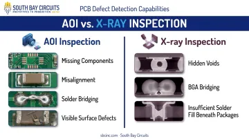
Use AOI and X-ray for anything complex or fine-pitch. AOI catches externally visible issues like missing parts, misalignment, and solder bridging well, but it can't see beneath a BGA package. That's where X-ray earns its keep, revealing hidden voids, bridging, and insufficient fill that no camera will ever catch (PICA Manufacturing's guide to AOI vs. X-ray inspection).
A few more habits worth locking in:
- Match your through-hole soldering method (wave, selective, or hand) to component sensitivity and board complexity
- Verify component orientation and polarity before reflow to avoid costly rework
- Clean boards thoroughly to remove flux residue, especially before conformal coating
Common Assembly Mistakes to Avoid
Most costly assembly problems trace back to a handful of repeat offenders:
- Incomplete or inconsistent BOM: Missing part numbers or vague specs force assemblers to chase down details, delaying production before it even starts.
- Skipped DFM/DFA reviews: It feels efficient upfront, but issues a review would have caught tend to resurface later as a costly respin.
- Design, fabrication, and assembly split across vendors: When something goes wrong, the finger-pointing starts, and nobody wants to own the problem, so the project stalls while blame gets sorted out.
This is the exact problem single-source manufacturing was built to solve. SBC controls design, fabrication, and assembly under one roof in Chandler, so there's no vendor handoff and no institutional knowledge lost between steps.
If a board doesn't perform, the same team that laid it out is the one troubleshooting it, with no blame game and no waiting on a third party to respond.
Frequently Asked Questions
How are PCBs assembled?
PCB assembly starts with applying solder paste through a stencil and placing components via pick-and-place or hand assembly. The boards then run through reflow or wave soldering, finishing with inspection and functional testing before shipping.
What is the difference between SMT and through-hole assembly?
SMT components mount directly onto pads on the board's surface, allowing for smaller parts and faster automated assembly. Through-hole components have leads that pass through drilled holes, creating a stronger mechanical bond for parts under physical stress.
How long does PCB assembly typically take?
Timelines vary widely based on board complexity, component availability, and order volume. Experienced single-source manufacturers like SBC can offer same-day or 3-day quick-turn options for qualifying projects alongside standard production schedules.
What is the most common defect in PCB assembly?
Common defects include solder bridging, missing or misaligned components, tombstoning, and cold joints. AOI catches most surface-visible issues, while X-ray reveals hidden defects beneath packages like BGAs.
Does successful assembly guarantee a fully working board?
Not on its own. Assembly quality matters, but design accuracy, component quality, and thorough functional testing all determine whether a board performs as intended once powered on.
Can the same company handle both prototype and high-volume PCB assembly?
Yes. SBC's in-house design, fabrication, and assembly capabilities allow a project to move from prototype straight into full production, without re-qualifying a new vendor or losing time to a handoff.