That mix-up isn't just a vocabulary problem. Ordering the wrong scope of work from a manufacturing partner can mean weeks of delay and thousands of dollars in wasted spend. This guide breaks down what a PCB actually is, what a PCBA is, how they differ, how one becomes the other, and how to pick a manufacturing partner who won't leave you managing that confusion yourself.
Key Takeaways
- A PCB is the bare board; a PCBA is that board fully loaded and ready to function.
- Layer count, material, and structure determine a PCB's cost and application fit.
- PCBA assembly relies on two core methods: SMT for density, THT for ruggedness.
- Testing requirements differ sharply between bare-board and assembled-board stages.
- Single-source manufacturers cut lead time and remove finger-pointing between vendors.
What Is a PCB (Printed Circuit Board)?
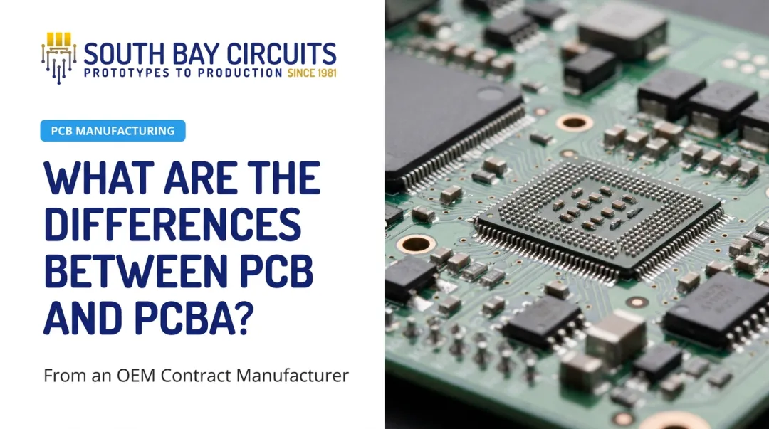
A PCB is the bare, non-conductive board that gives an electronic circuit its physical shape. It's typically built from FR-4 fiberglass, composite epoxy, or ceramic, then etched with copper pathways that carry electrical signals.
On its own, a PCB has no components and does nothing. It's a map, not a working circuit.
Every PCB shares a few core physical elements:
- Substrate – the rigid or flexible base material that holds everything together
- Copper layer/traces – etched pathways that define where current will flow
- Solder mask – the protective coating (often green) that insulates traces and marks solderable areas
- Silkscreen legend – printed text and symbols identifying part numbers, polarity, and logos
- Vias – plated holes that connect copper layers to each other
Think of a PCB as the skeleton of a circuit. It provides the blueprint for how current will eventually move once real components get attached.
Types of PCBs by Layer and Structure
Not all PCBs are built the same way. Layer count and construction change cost, weight, and where the board can be used.
By layer count:
- Single-sided – copper on one side only; cheapest option for simple devices
- Double-sided – copper on both sides, connected through vias
- Multilayer – three or more copper layers bonded with insulating material; standard in smartphones and laptops
By construction:
- Rigid – fixed shape; the most common PCB format
- Flexible – bends and folds into tight spaces; often built to IPC-6013 specs
- Rigid-flex – rigid sections joined with flexible connectors on one board
Layer count and material drive price and complexity. A two-layer board for a simple sensor costs a fraction of a 12-layer board built for aerospace or defense equipment.
For extreme environments, IPC publishes IPC-6012ES, an addendum for rigid boards that face vibration, thermal cycling, and ground testing in space and military use.
What Is a PCBA (Printed Circuit Board Assembly)?
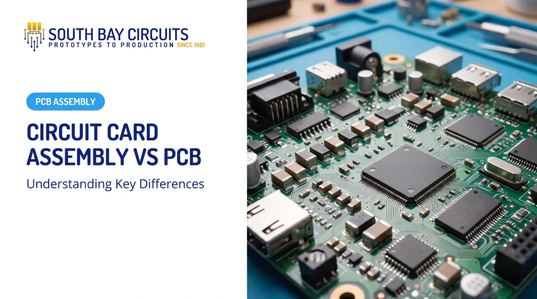
A PCBA is a PCB that's been fully populated with electronic components—resistors, capacitors, integrated circuits, and connectors—and soldered into a working assembly. Unlike a bare PCB, a PCBA is functional. It's ready to be dropped into a device and do its job.
One quirk that trips up newcomers: "PCBA" refers to both the process of mounting and soldering components and the finished product itself. You'll hear engineers say "we're running the PCBA now" and "the PCBA passed testing" in the same conversation, and both uses are correct.
From Bare Board to Working Assembly
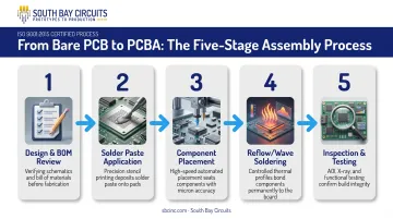
Turning a PCB into a PCBA follows this sequence:
- Design and BOM review – confirming the bill of materials matches the design files before production starts
- Solder paste application – stenciling paste onto pads where components will sit
- Component placement – automated pick-and-place machines position parts with precision
- Reflow or wave soldering – heat bonds components permanently to the board
- Inspection and testing – catching defects before the board moves downstream
SMT vs. THT: Choosing the Right Method
Two assembly methods dominate this stage, and the choice depends heavily on the end application.
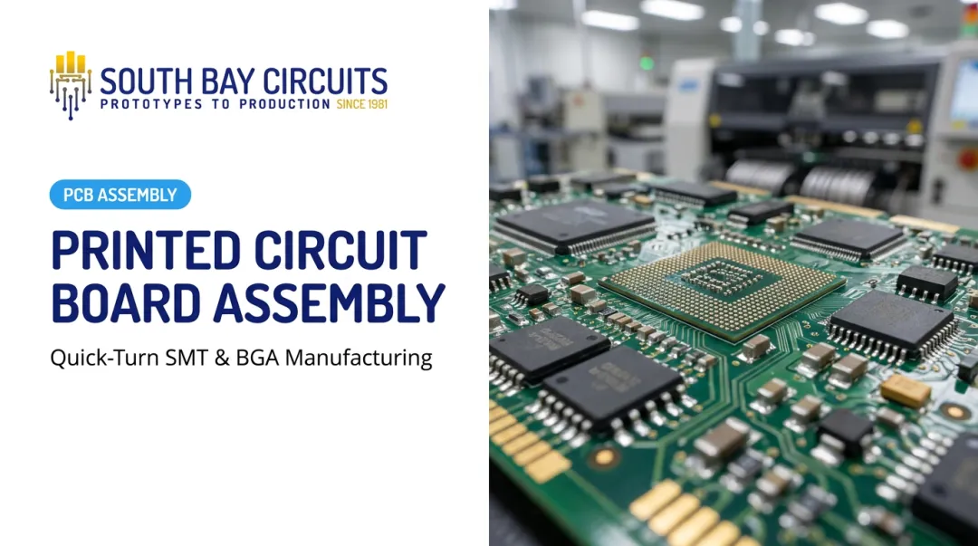
Surface-Mount Technology (SMT) mounts components directly onto the board surface and solders them via reflow. It supports higher component density and faster, more automated production, making it the go-to choice for compact, high-volume electronics.
Through-Hole Technology (THT) anchors leaded components through drilled holes, soldering them on the opposite side. This creates stronger mechanical bonds, which is why THT remains the preferred method for automotive and aerospace applications facing vibration and shock.
Whether a build uses SMT, THT, or both, assembly sits at the center of a massive industry. Grand View Research values the global PCBA market at $98.9 billion in 2025, projecting growth to $137.4 billion by 2033. That scale shows how central populated boards are to nearly every electronic product built today.
PCB vs. PCBA: Key Differences at a Glance
The distinction between a PCB and a PCBA isn't academic. It changes what you're actually buying.
| Factor | PCB | PCBA |
|---|---|---|
| State | Bare, unpopulated, non-functional | Populated, soldered, fully functional |
| Cost | Lower, no components or labor | Higher, includes parts, labor, equipment |
| Function | Structural/electrical foundation only | Performs the device's actual purpose |
| Testing | Continuity, lamination, hole quality | ICT, functional testing, AOI, X-ray |
| Sourcing | Fabrication-only vendors | Assembly-capable vendors (or both) |
Testing requirements illustrate the gap best. Bare-board testing checks continuity and hole integrity, often against standards like IPC-A-600 for board acceptability.
PCBA testing goes further, evaluating the board and every component together through in-circuit testing, automated optical inspection, and X-ray analysis for hidden solder joints under BGAs.
This matters for sourcing. Asking a vendor to quote a "PCB" versus a "PCBA" requests entirely different scopes of work, with different lead times, pricing structures, and equipment requirements. Get this wrong in a purchase order and you'll either receive a board that can't do anything, or an unexpected invoice for services you didn't plan for.
How a PCB Becomes a PCBA: The Manufacturing Journey
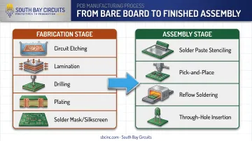
The path from design file to working assembly runs through two distinct stages.
Fabrication stage turns a digital design into a physical bare board:
- Circuit image transfer and etching define the copper pathways
- Lamination bonds layers together under heat and pressure
- Drilling creates holes for vias and components
- Plating makes those holes electrically conductive
- Solder mask and silkscreening finish the board's surface
Assembly stage populates that bare board with working parts:
- Solder paste stenciling prepares pads for components
- Pick-and-place machines position parts with speed and accuracy
- Reflow soldering bonds SMT components permanently
- Through-hole insertion and wave or hand soldering add any leaded parts
Quality control runs through both stages, not just at the end. Automated optical inspection, in-circuit testing, and functional testing catch defects before a board moves to final integration into a device.
Those checks only go so far when fabrication and assembly sit with different vendors. Every handoff is a chance for delays, miscommunication, or damage in transit. Files get lost in translation. Shipping adds days. And when a defect shows up, pinning down which vendor caused it turns into a blame game that stalls the project.
Why the PCB-to-PCBA Distinction Matters When Choosing a Manufacturing Partner
Plenty of manufacturers specialize in only one half of this process. Some only fabricate bare boards. Others only assemble boards fabricated elsewhere. That split forces customers to juggle two vendors, two shipping schedules, and two sets of quality standards. When something goes wrong, each vendor tends to point at the other.
South Bay Circuits (SBC) was built around avoiding exactly that problem. Founded in 1981, SBC has run integrated PCB fabrication and PCBA assembly under one roof at its 60,000-square-foot Chandler, Arizona facility since consolidating operations there in the early 2000s.
That structure means one team controls the process from bare board through finished assembly, removing the file transfers and shipping windows that slow down multi-vendor projects.
What that integration looks like in practice:
- PCB fabrication in as little as 24 hours
- Same-day PCBA assembly options for qualifying orders
- SMT, through-hole, and mixed-technology assembly, including fine-pitch placement down to 0.4 mm and BGA/micro-BGA work
- In-house AOI, X-ray, ICT, and functional testing across both fabrication and assembly stages
SBC also holds certifications that matter for regulated industries: ISO 9001:2015 (Certificate No. 10000903 QM15), AS9100 aerospace compliance, ISO 13485 for medical devices, and ISO/TS 16949 for automotive production.
For a defense contractor or medical device OEM, those credentials aren't paperwork. They're proof the same quality system governs every stage of the build.
A single-source model won't eliminate every manufacturing challenge. But it does simplify accountability, and it tends to shrink the total cycle time between prototype and full production, since there's no queue-and-ship gap between fabrication and assembly to manage.
Frequently Asked Questions
What does PCBA mean in electronics?
PCBA stands for Printed Circuit Board Assembly. It refers to both the process of soldering components onto a bare PCB and the finished, functional board.
How much does a PCBA cost?
Cost is driven mainly by layer count, component type and quantity, order volume, and whether you use SMT, through-hole, or mixed assembly. A firm number comes from your final BOM and design files.
Is a PCB the same thing as a PCBA?
No. A PCB is the bare, unpopulated board. A PCBA is that same board after components have been soldered on, making it fully functional.
What are the different types of PCBs?
The main types are single-sided, double-sided, multilayer, rigid, flexible, and rigid-flex. Each suits different levels of complexity and application demands.
How long does it take to go from PCB to a finished PCBA?
Turnaround depends on complexity and volume. With fab and assembly under one roof, single-source manufacturers often move from bare board to loaded assembly in days rather than the weeks multi-vendor handoffs can take.
What is the difference between SMT and through-hole assembly?
SMT mounts components directly onto the board surface, ideal for compact, high-volume production. Through-hole anchors leaded components through drilled holes, offering greater mechanical strength for rugged environments.