Every routing decision — trace width, via placement, plane continuity — directly affects signal integrity, EMI, manufacturability, and long-term reliability. That's true whether you're building an industrial sensor board or a flight-critical avionics module.
Many designers assume a clean schematic and solid component placement guarantee a working board. They don't. This guide covers the core routing rules, the mistakes that trip up even experienced engineers, and how the right manufacturing partner catches problems before they reach fabrication.
Key Takeaways
- Trace width, spacing, vias, and plane usage govern signal integrity and manufacturability together
- High-speed and differential signals demand controlled impedance, length matching, and minimal stubs
- Most routing failures trace back to broken return paths or skipped DFM checks, not bad tools
- Early fabricator involvement catches rule violations before they turn into production delays
What Is PCB Routing?
Routing is the physical implementation of your schematic's logical connections. Copper traces, vias, and planes across one or more layers turn a netlist into a working circuit.
The goal isn't just "connect A to B." Good routing delivers:
- Reliable signal transmission without reflections or excessive noise
- Adequate current delivery to every component without overheating traces
- Controlled electrical behavior, including impedance and timing, within limits your fabricator can actually build
Routing is not the same as placement. Placement decides where components sit on the board. Routing decides how they connect electrically. You can have perfect placement and still ruin signal integrity with careless routing. The reverse is also true, though bad placement makes clean routing nearly impossible.
Why PCB Routing Rules Matter
Routing rules exist because physics doesn't care how correct your schematic looks. Crosstalk, EMI, signal reflections, and voltage drops can all show up on a board that was designed "correctly" on paper but routed carelessly.
Skip routing discipline and you'll likely see:
- Timing violations on high-speed interfaces (USB, HDMI, Ethernet)
- Thermal hot spots from undersized traces
- Yield and reliability issues that surface during assembly, not design review
The Standards Behind the Rules
These rules aren't arbitrary. IPC-2221C, published in 2023, is the generic design foundation covering electrical clearance, impedance, and plane-clearance requirements. IPC-6012F governs qualification and performance for finished rigid boards, including multilayer constructions with blind and buried vias.
Industries layer on their own compliance demands: aerospace, medical, and automotive boards each carry additional regulatory weight beyond the generic IPC baseline.
What Happens When You Ignore Return Paths
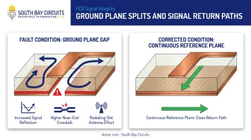
Signal Integrity Journal's split-plane testing showed what happens when a trace crosses a gap in the reference plane: measurable reflection, higher near-end crosstalk, and return current diverted into a radiating slot antenna.
That is a documented electrical consequence of a routing habit that is easy to fall into under deadline pressure.
Core PCB Routing Rules and Design Guidelines
These are the foundational rules every designer applies before tackling advanced, high-speed techniques. Get these wrong and no amount of clever stack-up design will save the board.
Trace Width, Spacing, and Current-Carrying Capacity
Trace width must match the current it carries. Too narrow, and resistive heating becomes a real problem. IPC-2152 is the dedicated standard for sizing conductors based on required current and acceptable temperature rise. It accounts for copper weight, board thickness, thermal conductivity, and nearby planes, not just amps.
Spacing matters just as much:
- Minimum spacing prevents crosstalk and shorts between adjacent traces
- Spacing requirements increase with both voltage and frequency
- Clearance (air path) and creepage (surface path) are separate calculations — pollution, humidity, and material choice all affect them
Don't eyeball trace width. Run the numbers through a trace-width/current calculator, then confirm the result against your fabricator's actual capability chart.
As a reference point, South Bay Circuits' capability chart lists standard trace-and-space at .004"/.004" for ½ oz external copper, with advanced tiers reaching .003"/.003" and .002"/.002". Heavier 2 oz copper jumps to .010"/.010" minimum. Match your design target to actual copper weight, not a generic assumption.
Via Types, Placement, and Best Practices
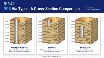
Multilayer boards use three common via types:
- Through-hole vias — run the full board thickness, simplest and cheapest
- Blind vias — connect an outer layer to an inner layer without passing through the whole stack
- Buried vias — connect internal layers only, invisible from either outer surface
Placement rules matter as much as via type selection:
- Keep adequate via-to-pad spacing to prevent solder wicking during reflow
- Via-in-pad designs need filled and plated vias — SBC's process uses non-conductive fill followed by plating directly over the filled via, which eliminates fan-out traces and shortens the signal path
- Use via stitching to tie ground planes together, which helps suppress EMI in RF and high-speed sections
For thermal vias, connect fully around the plated hole to the ground plane rather than through thin thermal-relief spokes. Masking them off can trap voids during soldering.
Ground and Power Plane Rules
Continuous, unbroken ground and power planes give return current a low-inductance path back to its source. Break that continuity and you invite trouble.
Routing a signal across a split plane forces return current toward the split edge, creating a longer, higher-inductance path. The result is increased EMI, crosstalk, and signal reflection, even when the trace itself looks perfectly routed.
Plane pairing in your stack-up helps here. Alternating signal and plane layers keeps a consistent reference plane under every routed signal, and adjacent power/ground plane pairs add interplane capacitance that smooths out power-bus noise.
High-Speed and Differential Pair Routing Rules
Controlled impedance routing means calculating trace geometry — width, spacing, dielectric height — against your stack-up to hit a target impedance value. IPC-2141A is the design guide covering microstrip, stripline, and differential/common-mode behavior, though it doesn't set interface-specific numbers.
Those numbers come from the interface itself:
| Interface | Differential Impedance Target | Notes |
|---|---|---|
| USB 2.0 | 90 ohms ±15% | Requires intra-pair length matching, solid reference plane |
| HDMI 1.4 (TMDS) | 100 ohms | Minimize stubs, trace length, and vias |
| Gigabit Ethernet (SGMII) | 100 ohms ±12% | 5-mil segment matching, 50-mil total channel matching |
Differential pair rules that apply across all three:
- Keep spacing consistent along the entire pair
- Route both traces on the same layer wherever possible
- Avoid sharp 90° bends — use gentler angles to reduce reflections
- Minimize stubs, since even short unterminated branches cause impedance discontinuities at high frequency
One misconception trips up a lot of designers: visually equal trace lengths don't guarantee equal propagation delay. Electrical length includes via transitions and pad entry, not just the copper run on the surface layer. Serpentine tuning should target time-of-flight, not ruler measurements.
Best Practices and Common PCB Routing Mistakes
Good routing starts before you draw a single trace.
Finalize placement first. Group related circuits together, isolate high-frequency sections from noisy digital logic, and confirm your stack-up. Placement quality drives routing efficiency. Trying to fix bad placement with clever routing rarely works.
Three mistakes show up again and again:
- Trusting the autorouter blindly: Early autorouters lacked signal-integrity constraints and often inserted excessive vias. Even modern tools need a manual design rule check (DRC) and DFM review before you call the layout done.
- Ignoring return paths: Splits and plane gaps under high-speed traces cause the EMI and crosstalk issues covered earlier.
- Skipping DFM checks entirely: Teams assume CAD default rules match what the fabricator can actually build.
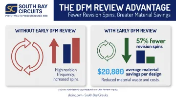
That last one costs more than most designers realize. An IPC-hosted DFM technical resource citing 2007 Aberdeen research found that advanced DFM users averaged 57% fewer revision spins and saved roughly $20,800 in materials per design compared to teams that skipped early DFM review. Those savings reflect the cost of one missed rule multiplied across a full production run.
Choosing a PCB Manufacturing Partner for Reliable Routing
Routing rules only matter if they match what your fabricator can actually produce. A design that looks perfect in your CAD tool but ignores real-world minimum trace/space, via specs, and tolerances leads straight to rework and schedule slips.
Validate against your fabricator's actual capability chart, not generic industry defaults:
- Minimum trace width and spacing by copper weight
- Via aspect ratios and microvia diameters supported
- Controlled impedance tolerance achievable in your chosen stack-up
South Bay Circuits has operated as a single-source PCB design, fabrication, and assembly partner since 1981. That continuity matters for routing because in-house DFM feedback happens before your board reaches the shop floor, catching rule violations while they're still cheap to fix.
Documented SBC capabilities include:
- Trace-and-space down to .002"/.002" at advanced process levels
- Hole aspect ratios up to 16:1
- Controlled-impedance tolerances as tight as ±5%, depending on process level
For regulated industries, certifications aren't just paperwork:
- ISO 9001:2015 covers fabrication, assembly, and box-build quality management
- AS 9100 compliance supports aerospace program requirements
- ISO 13485 compliance addresses medical device manufacturing
- ISO TS 16949 compliance supports automotive PPAP requirements on request
None of these certifications automatically rewrite your routing rules. They establish the quality framework your engineer's DFM review operates within. That review is still where split planes, undersized traces, and impedance mismatches get caught before fabrication starts.
Frequently Asked Questions
What is PCB routing?
PCB routing is the process of connecting components with copper traces based on the schematic's net list. It's distinct from placement, which determines where components physically sit on the board.
What is differential pair PCB routing and how is it used?
Differential pair routing uses two parallel, symmetric traces carrying complementary signals that cancel noise when read together. It's standard in USB, HDMI, and Ethernet interfaces, each with its own impedance target.
What is the standard trace width for PCB routing?
There isn't one universal standard width. Trace width depends on current, copper weight, and allowable temperature rise, and should be calculated per IPC-2152 guidance rather than assumed from a default value.
What's the difference between PCB routing and PCB layout?
Layout is the broader process, including component placement and stack-up design. Routing specifically refers to creating the copper trace connections between those placed components.
How does via placement affect PCB routing quality?
Poor via placement can create return-path discontinuities, plane voids, and localized thermal issues. Proper placement — including adequate via-to-pad spacing — maintains signal integrity and manufacturing reliability.
What are the most common PCB routing mistakes?
Routing signals over split planes, ignoring return-path continuity, and skipping manual DFM checks after auto-routing are the most frequent and costly mistakes designers make.