That's usually when the problem shows up: a trace runs hot under load, a signal degrades across a high-speed link, or a board fails in the field after passing every visual inspection. In aerospace, medical, and automotive applications, these failures aren't inconvenient. They're catastrophic.
This guide covers what traces actually are, how they're manufactured, how to size them correctly, and the design choices that separate a reliable board from a field failure waiting to happen. We'll also look at why the manufacturing partner you choose matters just as much as the layout itself.
Key Takeaways
- PCB traces are etched copper pathways that replace point-to-point wiring, carrying signals and power.
- Trace width and copper thickness must match current load and temperature rise, per IPC-2152.
- Impedance control, EMI mitigation, and length matching determine high-speed signal integrity.
- Copper weight and foil type (ED vs. RA) affect capacity, durability, and high-frequency performance.
- A certified, in-house manufacturing partner catches trace defects that generic fabrication misses.
What Are PCB Traces?
A PCB trace is a thin, flat conductive pathway, almost always copper, etched directly onto a circuit board's substrate. It connects components and carries electrical current or signals between them. Think of it as wiring that's been flattened, fixed in place, and printed with precision instead of hand-routed.
Traces do more than just connect point A to point B. They:
- Conduct signals between components and connectors
- Distribute power throughout the board
- Control signal timing and impedance in high-speed circuits
- Help dissipate heat away from critical components
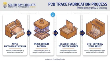
Traces are created through a photolithography and etching process:
- Applying a photosensitive film to the copper-clad substrate
- Imaging the film with the desired circuit pattern
- Developing away the unhardened resist to expose the copper underneath
- Etching off the exposed copper and stripping the remaining resist, leaving only the intended conductive paths behind
PCB Traces vs. Wires: What's the Difference?
This is one of the most common questions engineers new to PCB design ask, and the answer is straightforward.
Wires are round, flexible, standalone conductors that get manually routed and connected point-to-point. Traces, in contrast, are flat, fixed, and etched permanently onto the board's surface as part of the manufacturing process.
Traces replaced discrete wiring in modern electronics because they allow far greater miniaturization. A board that would require hundreds of hand-soldered wires can instead be etched with repeatable, predictable geometry in a single production step. No two wire harnesses are ever perfectly identical. Two boards etched from the same design file, however, are essentially the same board.
Types of PCB Traces: Signal, Power, and Ground
Not every trace on a board serves the same purpose, and that purpose dictates its sizing.
Signal traces are typically narrower and carry lower current, since their job is transmitting data or control signals rather than delivering power. Power and ground traces, by contrast, are wider, built to handle higher current-carrying needs without excessive heating or voltage drop.
Ground is frequently implemented not as a thin trace at all, but as a continuous copper plane, which provides a low-impedance return path and helps shield sensitive signals from interference.
How PCB Traces Are Manufactured: Materials & Copper Weight
Copper dominates PCB trace manufacturing for good reason. It offers excellent electrical conductivity and ductility, with enough tensile strength to etch cleanly into precise patterns using standard fabrication processes.
Copper weight, measured in ounces per square foot (oz/ft²), determines how much current a trace can carry and how well it handles heat. Heavier copper generally supports higher currents because it provides more cross-sectional area for current to flow through.
As a reference point, 1 oz/ft² of copper spread evenly corresponds to roughly 1.37 mils, or about 34.8 micrometers, of theoretical thickness. That said, copper weight and finished thickness aren't identical. Industry tolerances allow some variation between the nominal foil weight and what actually ends up on the board.
There are also two distinct types of copper foil used in PCB fabrication:
| Foil Type | Structure | Best Suited For |
|---|---|---|
| Electrodeposited (ED) | Vertical grain structure, rougher surface profile | Standard rigid boards; strong laminate adhesion |
| Rolled-annealed (RA) | Smoother surface, elongated horizontal grains | Flex PCBs; applications requiring ductility |
Foil smoothness directly affects high-frequency signal loss, not just overall manufacturing quality. Smoother copper reduces insertion loss at high frequencies because rougher surfaces amplify skin-effect losses as signal frequency climbs. If your design pushes into RF or high-speed digital territory, foil roughness is worth discussing with your fabricator before layout, not after.
At South Bay Circuits, this is exactly the kind of decision that benefits from in-house design and fabrication under one roof. When the same team handling your layout also runs the etching line, material selection questions get answered before they become production delays.

PCB Trace Width, Thickness & Current-Carrying Capacity
Getting trace width and thickness right matters more than most engineers assume until they've dealt with the alternative. Undersized traces overheat, degrade over time, and can eventually burn out entirely. Oversized traces aren't dangerous, but they waste board real estate and drive up material costs on high-volume runs.
The underlying physics is simple: current flowing through copper generates resistive heat, and that heat depends on the copper's resistivity, the trace's length, and its cross-sectional area (width multiplied by thickness).
The industry benchmark for this calculation is IPC-2152, IPC's standard specifically for determining current-carrying capacity in printed board design. It accounts for internal versus external conductors and acceptable temperature rise, superseding the older, more generic width-current charts many engineers grew up using. A single table simply can't account for every board's unique thermal environment.
A trace-width calculator is a reasonable starting point for early-stage design work. But for high-current or high-reliability applications, validate those numbers with your manufacturer's engineering team. A generic tool can't model how nearby copper planes or board mounting affect real-world heat dissipation.
Factors That Influence Trace Width Calculations
Before you can size a trace correctly, you need to know:
- Required current – the actual load the trace will carry
- Acceptable temperature rise – how much heating above ambient is tolerable
- Copper weight – sets the available cross-sectional area
- Ambient operating temperature – air versus vacuum, enclosure conditions
- Layer position – internal traces are surrounded by dielectric material and dissipate heat differently than external traces exposed to open air
Skipping any one of these inputs turns your width calculation into a guess.
Standard PCB Trace Thickness Considerations
Trace thickness generally scales with copper weight rather than board layer count alone. Single-sided, double-sided, and multilayer boards can all use the same copper weights. However, internal layers on multilayer boards face different heat-dissipation conditions than exposed outer layers, which affects how much current they can safely carry at the same thickness.
Rather than relying on generic thickness charts, confirm specifics against your fabricator's capability documentation. Copper weight options and finished thickness tolerances vary between manufacturers, and what one shop calls "standard" another may treat as a custom order.
Key Design Considerations for Reliable PCB Traces
Trace sizing solves the heat problem. Signal integrity is a different challenge entirely, and it's where a lot of high-speed designs run into trouble.
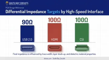
Impedance control matters because mismatched impedance causes signal reflections that corrupt data at high speeds. Target impedances are interface-specific, not universal.
USB 2.0 typically targets 90 ohms differential, while HDMI and CSI interfaces commonly target 100 ohms differential. Trace width and the dielectric properties of the board material both influence the final impedance, which is why impedance-controlled boards require tight coordination with your fabricator's stackup.
EMI mitigation relies on routing critical traces away from noisy components and maintaining continuous ground planes beneath high-speed signals. A split or interrupted return path underneath a fast-switching trace is one of the more common causes of unexpected emissions failures during compliance testing.
Crosstalk reduction comes down to spacing and geometry:
- Maintain adequate trace-to-trace spacing between high-speed and adjacent signal lines
- Use guard traces around especially sensitive signal paths
- Route differential pairs together and maintain consistent spacing along their full length
Trace length matching ensures synchronized high-speed digital signals arrive together at their destination. Skew tolerances differ by protocol. Some high-speed differential interfaces require much tighter length matching than others, which is why manufacturers set their own tolerance guidelines rather than applying one blanket number across every design.
Manufacturability best practices round out the list:
- Avoid sharp 90-degree bends; use 45-degree angles or curved routing instead
- Maintain uniform trace widths across a net wherever possible
- Respect minimum clearance rules, especially as copper weight increases, since thicker copper requires wider spacing during etching
- Coordinate annular ring and drill-to-copper clearances with your fabricator to avoid plating and reliability issues
None of these considerations exist in isolation. A board with perfect impedance control but poor crosstalk management will still fail signal integrity testing.
Common Trace Failures & Why Your Manufacturing Partner Matters
Even a well-designed layout can fail if fabrication introduces defects. The most common trace failure modes include:
- Overheating and burnout from undersized trace width relative to actual current load
- Corrosion from moisture ingress or ionic contamination bridging adjacent traces
- Delamination caused by moisture penetrating the board's layers, leading to inner-layer open circuits
- Etching defects, including over-etch that thins or fractures traces, and under-etch that leaves unintended copper bridging nets
Catching these problems before a board ships requires layered quality control, not a single inspection step:
- Automated optical inspection (AOI) flags visible opens, shorts, and pattern deviations
- Electrical testing verifies continuity and isolation across every net
- Impedance coupons, fabricated alongside the actual board using identical layer construction, confirm that controlled-impedance traces meet spec
- Microsection analysis cross-sections sample boards to evaluate laminate quality and plating integrity, catching defects no optical or electrical test can see
A single inspection method only sees one class of defect. High-reliability boards need all four working together.

This is where South Bay Circuits' background carries real weight. With over 40 years of PCB fabrication and assembly experience, SBC holds certifications including ISO 9001:2015, AS 9100, ISO 13485, and TS 16949. These credentials support customers in aerospace, medical, automotive, and industrial sectors, where trace failures simply aren't an option.
Because design, fabrication, and assembly all happen in-house at SBC's Chandler, Arizona facility, trace tolerances get controlled at every handoff. This eliminates the delays and miscommunication that come from juggling multiple vendors across a supply chain.
Frequently Asked Questions
What are traces in electronics?
Traces are thin copper conductive pathways etched onto a printed circuit board that carry electrical signals and power between components. They effectively replace traditional point-to-point wiring in modern electronics.
What is the difference between a wire and a trace?
A wire is a round, flexible, standalone conductor you connect manually between points. A trace is a flat copper pathway permanently etched onto the board's surface, enabling smaller and more repeatable circuit designs.
How do you calculate the correct PCB trace width for a given current?
You calculate trace width using current load, copper weight, and allowable temperature rise, typically referencing IPC-2152 guidelines or a trace-width calculator tool. For high-current or high-reliability designs, have a manufacturer's engineering team validate the result.
What is the standard PCB trace thickness?
Thickness varies based on copper weight and board type, whether single-sided, double-sided, or multilayer. Always confirm specifics against your manufacturer's capability sheet rather than assuming a universal standard.
What causes PCB traces to fail or overheat?
Common causes include undersized trace width relative to current load, corrosion from moisture exposure, manufacturing defects like over-etching, and poor thermal management in the overall board design.
Can a damaged PCB trace be repaired?
You can sometimes repair minor surface damage on accessible outer-layer traces using jumper wires or conductive ink. Internal or multilayer trace damage generally requires professional evaluation, since repair options become limited once a trace is buried.