Aerospace avionics and medical devices face a similar squeeze: more functions, tighter enclosures, higher stakes when something fails. Cram it all onto one monolithic PCB and you're setting yourself up for costly rework, painful debugging, and revision cycles that drag on for months.
Modular PCB design offers a way out. This guide covers what it means, the real benefits, a step-by-step implementation process, and how the right manufacturing partner keeps your modules moving instead of sitting in a shipping queue.
Key Takeaways
- Modular PCB design splits circuits into independently tested functional blocks, cutting rework and speeding revisions
- A "module" is a function; a "PCB" is the physical board that holds one or several
- Isolating analog, digital, and power sections improves signal integrity and simplifies debugging
- Standardized interfaces and version control avoid the coordination headaches modularity introduces
- Single-source manufacturing partners shorten the gap between validating one module and starting the next
What Is Modular PCB Design?
Modular PCB design means splitting a complex circuit into independent functional blocks, then designing, testing, and optimizing each one separately before bringing them together. Power regulation, communication, sensor interfaces, and processing each get treated as their own contained project with clearly defined inputs and outputs.
Compare that to traditional monolithic design, where the entire board is developed as one tightly coupled system. It works fine for simple circuits.
But once you're juggling RF sections, high-speed digital, and power conversion on the same layout, monolithic design becomes a bottleneck. Change one trace, and you risk breaking three other things, since every revision touches the whole board instead of one isolated piece.
Module vs. PCB: What's the Difference?
The terms get used interchangeably, but they're not the same thing.
- A module is a functional subsystem, such as power regulation or a communication interface, defined by what it does, not its physical form
- A PCB is the physical substrate that can host a single module or several modules side by side
Modules don't have to live on separate boards. A power regulation block and a communication block can sit on regions of the same PCB, wired together internally. Or they can be split across separate boards linked by connectors, cables, or a backplane, common in multi-board systems where mechanical constraints or repairability matter more than minimizing board count.
This distinction matters most in regulated industries:
- Aerospace and defense avionics, where AS9100-compliant processes govern how modules are documented and traced
- Medical electronics, where ISO 13485 compliance shapes how modules are validated before integration
- Automotive ECUs, where ISO/TS 16949 requirements apply to modular power and communication subsystems
- Industrial controls, where mixed board and module configurations need consistent quality documentation across suppliers
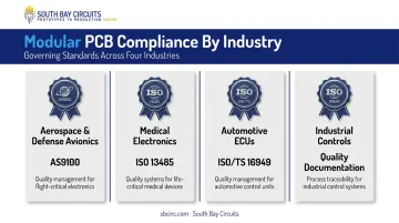
SBC holds all three certifications, which matters when a modular design needs to move from prototype to production without a compliance gap opening up during the handoff.
Key Benefits of Modular PCB Design
Splitting a design into modules pays off in ways that compound as the product gets more complex.
- Scalability without a full redesign: Add a new sensor or swap a protocol years into a product's life by updating one module, not the whole board. Critical for industrial controls and medical devices with decade-long production runs.
- Faster fault isolation: A break on a monolithic board means tracing signals across the entire layout. Modular design narrows debugging to a single block, turning guesswork into a shortlist.
- Reuse that saves engineering hours: A validated power supply or communication interface doesn't need reinventing for every new project. Reusing proven circuits cuts redundant engineering work and the errors that come with starting from scratch.
- Quicker prototyping and NPI cycles: Revise one module, retest it, and move on, without rerunning validation on the whole board every time a spec changes.
- Genuine parallel development: Multiple engineers can own different modules at once, so one handles power while another works the RF front-end, independently.
- Better signal integrity and thermal behavior: Analog Devices' mixed-signal layout guidance recommends separating sensitive analog circuitry from noisy digital sections, exactly the isolation modular partitioning provides. It also keeps a power block's heat and switching noise from bleeding into sensitive areas.
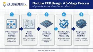
Step-by-Step Modular PCB Design Process
Step 1: Define Functional Units and Interfaces
Start by grouping circuitry by function: power, processing, communication, and sensors. Base these groupings on signal flow, power distribution, and physical constraints. Then lock down how those blocks will talk to each other, including:
- Connector types and pin assignments
- Signal protocols and voltage levels
- Mechanical footprint and keep-out zones
Get this wrong early, and you'll be renegotiating interfaces after layout has already started.
Step 2: Create Modular Schematics
Build each module as its own schematic sheet, linked through a parent hierarchy rather than dumped into one flat drawing. Altium Designer, KiCad, Cadence Allegro, and Zuken all support hierarchical, multichannel schematic capture, meaning repeated circuit blocks get instantiated once and reused, not redrawn.
Step 3: Design and Layout Each Module
Lay out each module with its own priorities: signal integrity for high-speed digital, EMI shielding for RF sections, thermal management for power conversion. Decide early whether modules will share one physical board or live on separate boards connected by a backplane or cable assembly. That call shapes stackup, placement, and connector choice.
Step 4: Prototype, Test, and Validate Independently
Test each module on its own before it sees the rest of the system. For example, validating a power supply module independently through load testing, thermal checks, and ripple measurement surfaces problems while they're still cheap to fix. Waiting until full-system integration risks hiding that same fault anywhere in the design.
Step 5: Integrate, Validate, and Prepare for Production
Once every module checks out, combine them and run full-system testing. Verify inter-module interactions, since even validated blocks can create new signal integrity or power issues once connected. Then generate DFM-ready files, including Gerbers, drill files, and BOM, for fabrication and assembly. Partnering with a single-source contract manufacturer, such as South Bay Circuits, keeps this handoff smooth, since design, fabrication, and assembly happen under one roof, from prototype through full production runs.
When Should You Use a Modular Design Approach?
Modular design isn't the right call for every board. It earns its keep in specific situations.
Embedded systems with distinct functions. If a product handles sensing, communication, and a user interface as clearly separate tasks, modularity lets teams develop and test each one in parallel instead of standing in line behind each other.
Multi-board systems. When power, processing, and communication are split across interconnected boards, common in industrial controls and automotive platforms, modular thinking keeps each board manageable on its own.
Automakers face this tradeoff directly. EE Times reported that adding a dedicated ECU for every new vehicle feature increases weight, component count, and troubleshooting effort. That's why manufacturers now consolidate functions into fewer, more capable modules instead of piling on more boards.
Mixed-signal designs. Boards combining sensitive analog circuitry with noisy digital logic benefit from physical and electrical isolation between sections. Modular partitioning gives designers a natural boundary to enforce that separation.
Outside these scenarios, if a board is simple, low pin count, and unlikely to change, monolithic design is still faster and cheaper. Modularity earns its complexity when the product itself is complex.
Common Challenges in Modular PCB Design
Modular design solves real problems, but it introduces a few of its own.
More upfront design effort. Partitioning a system into modules and defining clean interfaces takes more planning than starting layout right away. Prioritize high-reuse modules first: power supplies and communication interfaces show up in nearly every project, so getting those right pays off across multiple products.
Compatibility issues between modules. Different form factors or mismatched interfaces between modules can turn integration into a scavenger hunt for adapter boards. A documented interface specification covering connector types, pinouts, voltage levels, and protocols heads this off before it becomes a layout problem.
Coordination across design teams. When multiple engineers own different modules, it's easy for someone to build against an outdated revision of another team's block. Version control systems and regular cross-team design reviews catch this before it turns into a respin.
Here's how these three challenges map to their fixes:
| Challenge | Mitigation |
|---|---|
| More upfront design effort | Prioritize high-reuse modules (power, comms) first |
| Compatibility issues between modules | Standardized connectors, documented interface spec |
| Coordination across design teams | Version control, scheduled cross-team reviews |
None of these are dealbreakers. They're the cost of doing modularity right instead of doing it halfway.
Partnering with SBC for Modular PCB Design-to-Production
Validating modules independently only pays off if your manufacturing partner can turn each one around fast. Bouncing a design between a layout house, a separate fab shop, and a third-party assembler adds queue time and shipping days at every handoff, exactly the delay modular design is supposed to eliminate.
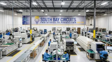
South Bay Circuits runs design, fabrication, assembly, and box build under one roof at our 60,000-square-foot Chandler, Arizona facility. That single-source model means a module moves straight from layout to bare board to loaded assembly instead of sitting in a shipping box between steps.
Speed matters when you're testing several modules before committing to full-system integration:
- PCB fabrication in as little as 24 hours
- Same-day assembly options for time-sensitive prototype runs
- Complete control of the process from design through production, so nothing gets lost between vendors
For regulated industries, certifications carry as much weight as speed. SBC holds a full slate of industry credentials:
- ISO 9001:2015 for quality management
- AS9100 for aerospace programs
- ISO 13485 compliance for medical devices
- ISO/TS 16949 for automotive electronics
- IPC-6012 Class III and MIL-PRF-31032 for military-grade boards
A modular design built for an avionics system or a medical device doesn't hit a compliance gap moving from prototype to production.
Founded in 1981, SBC has spent over four decades refining that single-source approach, long enough to know that the fastest path to a working system is validating each piece before committing to the whole.
Frequently Asked Questions
What is a modular PCB?
A modular PCB is a board designed using independent, functional blocks, such as power, communication, or sensing, that are developed and tested separately before integration into the complete system. It's a design methodology, not a different type of physical board.
What is the difference between a module and a PCB?
A module is a functional subsystem, like power regulation or a communication interface. A PCB is the physical board itself, which can host a single module or several modules together.
When should I use modular PCB design instead of a single-board design?
Modular design fits embedded systems with distinct functions, multi-board systems splitting power and processing across connected boards, and mixed-signal designs needing isolation between analog and digital sections.
What PCB design software supports modular design?
Altium Designer, KiCad, Cadence Allegro, and Zuken all support hierarchical, multichannel schematic capture, letting you build and reuse modules as linked sheets instead of one flat schematic.
Does modular PCB design increase manufacturing cost?
It can add connector and board costs when functions are split across multiple physical boards. That's usually offset by reduced rework and faster debugging, since isolated faults are cheaper to fix than system-wide ones.
How does modular design impact new product introduction (NPI) timelines?
Independently validated modules let you catch problems early instead of during full-system integration. Paired with a manufacturing partner offering same-day to 3-day quick-turn, that shortens the overall path from prototype to production.