Introduction
Every PCB project starts with the same balancing act: cost versus board space versus circuit complexity. For many designs, that balancing act lands on the same answer: the 2-layer double-sided PCB.
Get the layer count wrong and you either overpay for capability you don't need, or you hit a wall trying to route traces that have outgrown a single copper layer. Many engineers also run into a smaller, more annoying problem: is a "2-layer" board the same thing as a "double-sided" board, or something different?
This guide clears that up. It covers what a 2-layer double-sided PCB actually is, how it's manufactured, and where it earns its reputation as the industry's dependable middle ground. You'll also see how it compares to single-sided and multilayer boards, where it shows up in real products, and what to look for when picking a fabrication partner.
Key Takeaways
- 2-layer and double-sided PCBs are the same board: copper on both faces, linked by plated through-holes, no internal layers.
- Routing area roughly doubles versus single-sided boards, without multilayer lamination costs.
- Double-sided fabrication typically costs 35–40% more than single-sided—still well under multilayer pricing.
- Ideal for moderate-complexity designs; high-speed, RF, or controlled-impedance work needs multilayers.
- IPC-6012 and IPC-2221 set the quality and design rules regulated industries rely on.
What Is a 2-Layer Double-Sided PCB Board?
A 2-layer double-sided PCB has conductive copper on both the top and bottom of a single insulating substrate. No inner copper layers sit between those two faces.
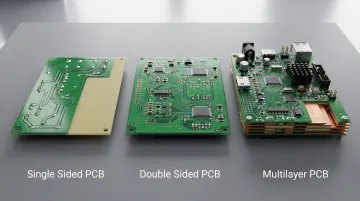
How it compares to other stackups:
- Single-sided: Copper on one face only
- 2-layer / double-sided: Copper on top and bottom, no inner layers
- Multilayer: Three or more copper layers with dielectric between them
The two copper faces connect through plated through-holes (PTHs). Fabricators drill a hole through the board, then plate the barrel with copper so current can travel from top to bottom along the hole wall.
Without that plating, the two copper layers would be separate, disconnected circuits sharing a substrate.
"2-layer" and "double-sided" describe the same board. The two layers are the top and bottom copper. Spec sheets may favor one label over the other, but the construction is identical either way.
Key Structural Elements
The base material is almost always FR4, a fiberglass-reinforced epoxy laminate faced with copper foil on both sides. Copper weight is a real current-capacity decision, not a default checkbox:
- 1 oz copper on a 1mm-wide external trace handles roughly 2 to 2.5 amps before a 10°C temperature rise.
- 2 oz copper on that same trace jumps to around 4.2 amps under the same conditions.
That's not a universal rating. Ambient temperature, trace location, and allowed temperature rise all shift the numbers, but it illustrates why copper weight is a real design decision, not an afterthought.
Solder mask and silkscreen legend go on both faces too. The mask protects copper from oxidation and solder bridging; the silkscreen marks outlines, reference designators, and polarity so parts are identified and oriented correctly at assembly.
Component Placement Flexibility
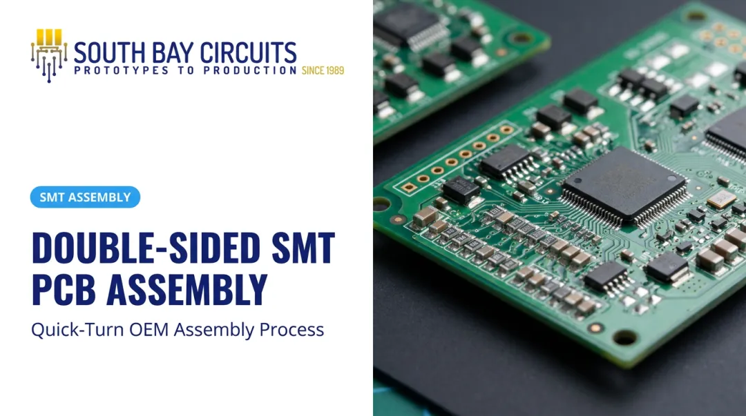
Because both sides carry copper, both sides can carry components. SMT parts, through-hole parts, or a mix of both can populate the top and bottom of the board. That flexibility increases component density without forcing a jump to multilayer construction, which is exactly why so many mid-complexity designs stop here.
How 2-Layer Double-Sided PCBs Are Manufactured
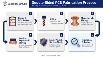
The process largely mirrors single-sided fabrication, with added steps for imaging, drilling, and plating both conductive layers instead of one. Here's the general sequence:
- Design and DFM review — Trace widths, spacing, and hole sizes get checked against manufacturability rules before anything touches production. Fine-line designs can push trace and space down to 0.003 inches with engineering review; standard builds typically hold to 0.004 inches on half-ounce copper.
- Drilling — Holes are mechanically drilled at every location where the top and bottom layers need to connect.
- Through-hole plating — Electroless copper deposits on the drilled hole walls first, since fiberglass isn't conductive. Electrolytic copper plating then builds up that layer to create a solid, conductive plated-through-hole.
- Imaging, exposure, and etching — Photoresist film goes onto both sides at once. UV exposure hardens the circuit pattern, and etching strips away the unwanted copper, leaving the final trace layout on each face.
- Solder mask, legend, and surface finish — Both sides get solder mask and silkscreen, followed by a surface finish such as ENIG or lead-free solder to protect exposed copper and keep it solderable.
- Inspection and testing — Automated optical inspection checks registration accuracy, and electrical continuity testing confirms there are no opens or shorts. The panel is then routed or scored before packaging.
Through-hole plating is the most technically demanding step in double-sided fabrication. Void-free, well-adhered PTH walls determine whether layer-to-layer connections hold up in the field.
A hole with incomplete plating can pass a quick visual check and still fail months later. Serious process control means daily cross-section analysis on test coupons—hole integrity, plating thickness, and registration checked on every panel, not occasional spot checks.
Advantages and Limitations of 2-Layer Double-Sided PCBs
Key Advantages
Double-sided construction roughly doubles available routing area compared to a single-sided board. That extra room lets designers fit denser circuits without paying for a multilayer stackup they don't actually need.
Cost sits in a sensible middle ground too. One widely cited fabrication cost model puts the jump from one layer to two layers at roughly 35-40%, with a similar increase moving from two layers to four. That means double-sided boards cost meaningfully more than single-sided, but far less than jumping straight to multilayer.
Manufacturing is also simpler than multilayer production:
- No internal lamination cycles to manage.
- No layer-to-layer registration between buried copper planes.
- Fewer process steps overall, which typically supports faster turnaround.
Limitations to Consider
Double-sided boards are more complex to produce than single-sided ones, mainly because of the drilling and plating requirements discussed earlier. Via defects tend to show up most often with fabricators who have limited PTH experience, so shop capability matters more here than the spec sheet suggests.
Heat and electromagnetic interference are two other concerns. Densely populated double-sided designs concentrate heat in a small footprint, and without a deliberate ground plane strategy, EMI can become a problem fast.
Industry guidance on this point is direct: route signals and power on one side while keeping the other side substantially intact as a ground-reference plane. Gaps or crossings in that return path let electromagnetic fields leak into places they shouldn't be.
Finally, double-sided boards simply aren't built for everything. High-speed signals, RF applications, and designs that require controlled impedance or dedicated power/ground planes outgrow what two copper layers can deliver. That's where multilayer construction takes over.
Double-Sided vs. Single-Sided vs. Multilayer PCBs
| Attribute | Single-Sided | Double-Sided (2-Layer) | Multilayer |
|---|---|---|---|
| Layer count | 1 copper layer | 2 copper layers | 3+ copper layers |
| Component mounting | One side only | Both sides | Both sides, multiple planes |
| Circuit complexity | Basic | Moderate | High |
| Relative cost | Lowest | ~35-40% more than single-sided | ~35-40% more than double-sided |
| Typical applications | Simple consumer devices, basic sensors | Consumer electronics, power supplies, industrial controls | RF systems, high-speed digital, controlled-impedance designs |
Choose double-sided over single-sided when a design needs more routing area, or needs components on both faces, but doesn't require advanced signal integrity control. It's the natural upgrade path once a single-sided layout runs out of room.
Upgrade to multilayer when you're dealing with high-speed signals, RF circuitry, or any design that needs controlled impedance and dedicated power and ground planes. Trying to force those requirements onto two copper layers usually causes more problems than it solves.
Industries and Applications of 2-Layer Double-Sided PCBs
Double-sided boards show up across a wide range of moderately complex products:
- Consumer electronics — general-purpose devices where cost control matters as much as performance.
- LED lighting and power supplies — power conversion circuits that benefit from two-sided routing without needing multilayer planes.
- Automotive control modules — subsystems within larger vehicle electronics architectures.
- Industrial instrumentation — control and monitoring equipment built for durability over decades of service.
- Telecom and networking equipment — phone systems and related infrastructure hardware.
Regulated industries use double-sided boards too, usually as simpler subsystems inside larger certified assemblies.
South Bay Circuits (SBC), a Chandler, Arizona contract manufacturer since 1981, builds double-sided PCBs for medical, aerospace and defense, automotive, and industrial customers. That work is backed by ISO 13485, AS 9100, ITAR registration, and ISO/TS 16949 compliance.
Quality compliance in these sectors isn't optional. IPC-6012 (revision F) sets qualification and performance standards for rigid PCBs, including double-sided construction. IPC-2221 covers the generic design rules that apply to single-sided, double-sided, and multilayer boards alike.
For a medical device manufacturer or defense contractor, meeting these standards is the baseline for product approval.
Choosing the Right 2-Layer Double-Sided PCB Manufacturing Partner
Not every fabricator handles PTH and copper plating with the same consistency. When evaluating a partner, look for:
- Demonstrated PTH and plating experience, since this is where double-sided defects most commonly originate.
- In-house DFM support that catches trace, spacing, and hole-size issues before production starts, not after a failed board comes back.
- Relevant quality certifications such as ISO 9001, ISO 13485, AS9100, or ITAR registration, depending on your industry.
Single-source fabrication-to-assembly capability matters more than it first appears. When one vendor builds the bare board and another handles assembly, a defect leaves you chasing accountability between two companies. A single-source model removes that friction.
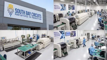
South Bay Circuits (SBC) operates on that model from a 60,000+ square foot Chandler, Arizona facility. The company holds ISO 9001:2015 certification (Certificate No. 10000903 QM15, valid through 2027), along with ISO 13485, AS9100, and ITAR registration.
Under one roof, SBC handles PCB design, layout, fabrication, and assembly, including double-sided SMT electrical testing via clamshell fixtures, for medical, aerospace, automotive, and industrial customers.
If you're weighing a double-sided PCB project, request a DFM review or quote before committing to production. One extra day can surface cost and turnaround issues while they're still cheap to fix.
Frequently Asked Questions
What is a double-sided PCB board?
A double-sided PCB has conductive copper layers on both the top and bottom of a single substrate, connected by plated through-holes. It has no internal copper layers, unlike multilayer boards.
What's the difference between a 2-layer PCB and a double-sided PCB?
There isn't one. Both terms describe the same board construction, since the "2 layers" simply refer to the top and bottom copper sides.
How much do double-sided PCBs cost compared to single-sided boards?
Double-sided boards typically cost around 35-40% more than single-sided boards due to added drilling and plating steps. They remain significantly cheaper than multilayer construction.
What materials are commonly used for double-sided PCBs?
FR4 is the standard substrate for most double-sided boards. Specialized applications sometimes use rigid polyimide for added thermal stability.
How long does double-sided PCB fabrication typically take?
Standard lead times vary with complexity and order volume, often running around five working days for pooled production runs. Quick-turn providers can deliver eligible projects in as little as 24 hours; SBC offers same-day to multi-day quick-turn schedules from its Chandler, AZ facility.
Can double-sided PCBs handle high-frequency or high-speed designs?
Double-sided boards work well for moderate-speed applications, but high-speed, RF, or controlled-impedance designs generally require multilayer construction. Two copper layers can't provide the dedicated reference and power planes those applications need.