Many manufacturers still treat testing as a final checkpoint rather than a continuous discipline built into every stage of production. That gap shows up later, in warranty claims, field returns, or regulatory audits, when it's far more expensive to fix.
This guide breaks down what PCB and PCBA reliability testing actually involves, the standards that govern it, and how a structured, step-by-step approach protects quality, compliance, and uptime across the product lifecycle.
Key Takeaways
- PCB testing checks the bare board; PCBA testing evaluates the assembled circuit under real-world stress.
- Test methods span electrical (ICT, flying probe), inspection (AOI, X-ray), and environmental (thermal cycling, HALT/HASS).
- IPC-A-610J, J-STD-001J, and IPC-9701B set current acceptability and test benchmarks for 2024-2025 production.
- Production volume, design maturity, and end-use environment determine the right test mix.
What Is PCB and PCBA Reliability Testing?
PCB reliability testing examines the bare, unpopulated board, checking traces, lamination, and layer-to-layer isolation before a single component gets soldered on. PCBA reliability testing goes further, evaluating the fully assembled board under electrical, mechanical, and environmental stress once components are in place.
Both play distinct roles across the manufacturing lifecycle:
- Incoming quality control – verifying bare boards meet spec before assembly begins
- New product introduction (NPI) – validating a design's manufacturability and durability before scaling up
- Design qualification – proving a board meets its intended use-case requirements
- Ongoing production monitoring – catching process drift before it becomes a field problem
Across every stage, testing methods fall into three categories:
- Electrical/functional – confirms the circuit works as designed
- Inspection-based – finds visible or hidden physical defects
- Environmental/destructive – simulates years of real-world stress in days or weeks
None of these alone tells the whole story. A board can pass electrical testing and still carry a latent solder fatigue risk that only shows up under thermal cycling.
Why PCB/PCBA Reliability Testing Is Critical for Manufacturers
Rigorous testing reduces operational risk, keeps regulatory auditors satisfied, and protects long-term product performance in sectors where failure isn't an option.
Catching Defects Before They Reach the Field
Solder voids, opens, shorts, and tombstoning are common assembly defects, and most are far cheaper to fix on the production floor than after shipment. Once a defective board reaches the field, the cost stacks up: completed-board rework, retesting, failure analysis, production interruption, replacement logistics, and field-service labor.
There's no universal industry multiplier that applies cleanly to every PCB or PCBA defect. What's consistent is the direction: escaped defects almost always cost more than the ones caught on the line, through the sheer volume of downstream steps they touch.
Supporting Compliance Frameworks
That cost math is only part of the picture. Reliability testing is also a contractual and regulatory requirement:
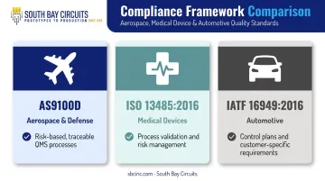
| Framework | Governs | What It Requires |
|---|---|---|
| AS9100D | Aerospace, space, defense | Risk-based, traceable QMS processes across the supply chain |
| ISO 13485:2016 | Medical devices | Process validation, risk management, and full traceability |
| IATF 16949:2016 | Automotive | Control plans and customer-specific test requirements |
South Bay Circuits holds ISO 9001:2015, AS9100, and ISO 13485 compliance, aligning its qualification process with these frameworks. Even rigorous programs face field risk, though: MedTech Dive reported that a ResMed ventilator safety issue linked to five serious injuries stemmed from a leaking component that damaged PCBA circuitry and triggered a fail-safe state. It's a reminder that environmental interactions, not just workmanship defects, can compromise an assembly in the field.
Building Trust Through Documented Process
Beyond compliance, a repeatable, documented reliability process builds customer confidence. It also shortens NPI (New Product Introduction) cycles: catching a design or process issue during qualification, rather than after a production run, saves rework and scrap without slowing the schedule down.
Common PCB/PCBA Reliability Testing Methods and Standards
Reliability testing splits into three complementary categories: electrical/functional, inspection-based, and environmental/stress. Each catches failure modes the others miss.
Electrical and Functional Testing
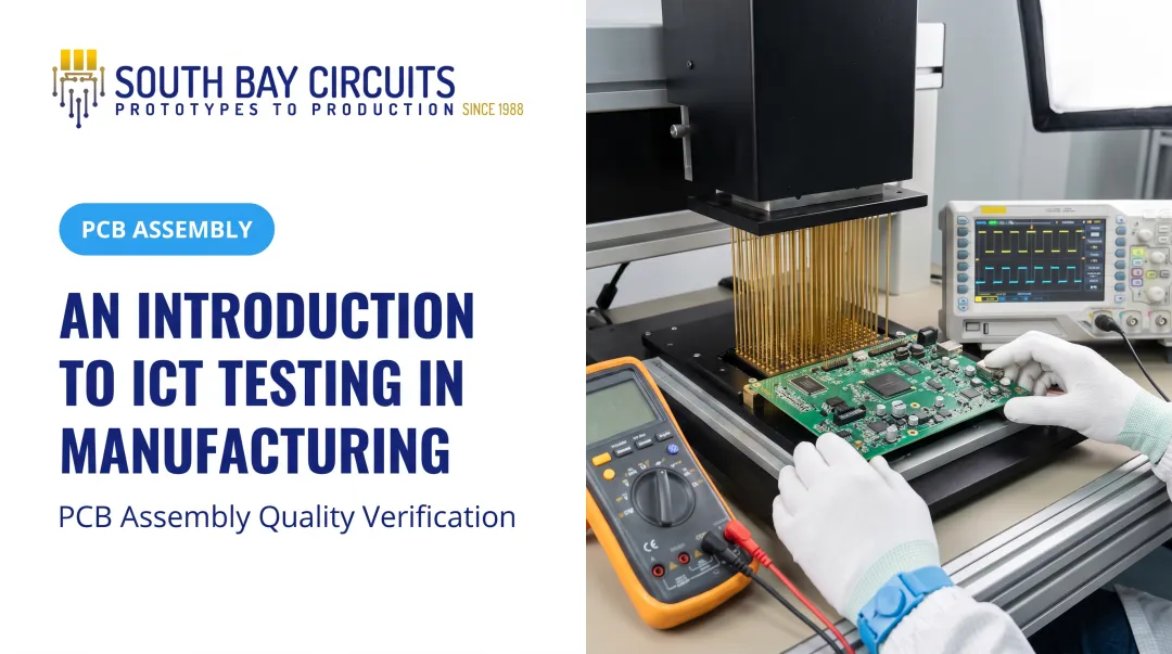
In-Circuit Test (ICT) uses a custom "bed of nails" fixture to contact multiple test nodes simultaneously, checking for shorts, opens, and correct component orientation. It's fast and repeatable, making it the go-to for high-volume, mature designs, though the fixture investment only pays off at scale.
Flying Probe Test uses programmable, moving probes instead of a fixed fixture, checking opens, shorts, resistance, and capacitance node by node. It's slower per unit than ICT but far more flexible, ideal for prototypes and low-to-medium volume runs where designs still change.
Inspection-Based Testing
Automated Optical Inspection (AOI) uses high-resolution imaging to catch solder bridges, tombstoning, and placement defects visible on the board's surface. X-ray Inspection (AXI) reveals hidden defects, like BGA voids, barrel cracks, and internal solder joint issues, that no camera can see from the outside.
Neither replaces the other. AOI checks what's visible; AXI checks what's buried under a package.
Environmental and Accelerated Stress Testing
Thermal cycling per IPC-9701B (2022) characterizes fatigue life in surface-mount solder attachments by repeatedly stressing the board between temperature extremes. Duration depends heavily on ramp rate, dwell time, cycle count, and monitoring approach, so there's no fixed timeline that applies to every board.
HALT pushes a design past its normal limits using combined thermal and vibration stress to find where it actually breaks, useful during design qualification, not production screening. HASS applies a lighter, production-derived version of that same stress to catch process defects without consuming the product's useful life.
Standards That Govern PCBA Testing and Inspection
| Standard | Current Revision | Scope |
|---|---|---|
| IPC-A-610 | J (2024) | Visual acceptability criteria for assemblies |
| J-STD-001 | J (2024) | Soldering process and material requirements |
| IPC-9252 | B (2016) | Electrical testing of unpopulated bare boards |
| IPC-TM-650 | Method-specific | Individual test method procedures (cite the specific method number) |
Industry-specific requirements, like AS9100, ISO 13485, or ITAR, layer additional documentation and traceability requirements on top of these baseline standards, depending on the end application. South Bay Circuits holds all three certifications, building that documentation trail into aerospace, medical, and defense programs from day one.
How PCB/PCBA Reliability Testing Works – Step by Step
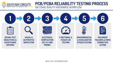
Most reliability programs break down into six practical stages. Skipping any of them erodes the value of the testing investment. Common missteps include:
- Skipping baseline documentation before testing begins
- Rushing environmental simulation to save schedule time
- Failing to close the loop on corrective action
Define test objectives and acceptance criteria. Identify the applicable IPC class, end-use environment, and specific failure modes, such as thermal fatigue in automotive modules or shock resistance in defense electronics, before board fab begins. This alignment prevents disputes later.
Run visual and automated inspection. AOI and manual inspection against IPC-A-610 criteria catch solder and placement defects early, when they're cheapest to fix.
Verify electrically with ICT or flying probe. Confirm continuity, isolation, and component orientation against the schematic and netlist before moving to more expensive stress testing.
Perform functional and power-on testing. Validate that the board actually does its job under rated voltage and load, not just that it's wired correctly.
Apply environmental and accelerated stress testing. Thermal cycling, vibration, or HALT/HASS exposure, matched to the deployment environment, predicts long-term durability that electrical tests alone can't reveal.
Document failures and drive corrective action. X-ray or microsection analysis on any failures, combined with logged root causes, feeds directly back into design and process improvements. Skipping this step means repeating the same mistakes on the next build.
How South Bay Circuits Supports Reliable PCB and PCBA Manufacturing
South Bay Circuits has operated as a single-source PCB fabrication and assembly partner since 1981, serving aerospace, medical, automotive, and defense customers from a 60,000-square-foot facility in Chandler, Arizona.
The company holds ISO 9001:2015 certification, ISO 13485 compliance for medical device production, ISO TS 16949 compliance for automotive, and AS9100 compliance for aerospace work, alongside ITAR registration and CMMC Level 1 status for defense programs.
That single-source model matters for reliability testing specifically:
- In-house electrical and inspection testing – ICT, an ATG A5CF Flying Probe system, AOI, and a Glenbrook X-ray system all operate under one roof, alongside burn-in, hi-pot, and vibration testing
- 100% inspection coverage – bare boards are visually inspected to IPC-600 Class II/III, and assemblies to IPC-610 Class II/III
- Full-process traceability – an ERP system tracks components and process data from incoming material through final shipment
- Fast iteration cycles – layout-to-loaded-assembly in as little as 48 hours, with 24-hour bare board fabrication and same-day to 3-day assembly turnaround
Keeping design, fabrication, assembly, and testing under one roof eliminates the finger-pointing that happens when a defect surfaces and three vendors each blame the other. It also means test iterations don't sit in a shipping queue between steps, which can add more delay than the actual testing itself.
Ultimately, effective reliability testing evolves with every product generation, refined by what the last build's failure data actually showed you.
Frequently Asked Questions
What is PCBA reliability testing?
PCBA reliability testing evaluates an assembled board's ability to withstand electrical, thermal, and mechanical stress over its expected service life. It combines electrical verification, inspection, and environmental stress testing.
What is PCBA testing?
PCBA testing broadly covers inspection, electrical verification, and functional checks performed after component assembly. The goal is confirming build quality before the board ships or moves to the next production stage.
What are the PCBA inspection standards?
IPC-A-610 sets visual acceptability criteria, J-STD-001 governs soldering requirements, and IPC-TM-650 provides standardized procedures for individual test methods. Both IPC-A-610 and J-STD-001 are currently on Revision J (2024).
What is the difference between PCB and PCBA reliability testing?
PCB testing focuses on the bare board, checking traces, lamination, and layer isolation before assembly. PCBA testing evaluates the fully populated, soldered assembly under electrical and environmental conditions.
How long does PCBA reliability testing typically take?
Timelines vary widely by test type. Flying probe testing can run anywhere from 35 seconds to 28 minutes depending on net count. Environmental stress testing under IPC-9701B can take days to weeks, depending on the thermal profile and cycle count.
Which industries require the most rigorous PCBA reliability testing?
Aerospace, medical devices, automotive, and defense sectors carry the strictest reliability and documentation requirements, driven by frameworks like AS9100, ISO 13485, and IATF 16949. A single field failure in these applications can mean safety incidents, not just warranty costs.