Introduction
PCB assembly is the process of populating a bare circuit board with electronic components and permanently bonding them using molten solder. That single sentence covers a manufacturing step that determines whether a device works for ten years or fails in ten weeks.
This guide is written for design engineers, procurement teams, and OEMs in aerospace, medical, automotive, and industrial sectors. For these industries, a weak solder joint threatens safety, reliability, and regulatory compliance, not just appearance.
Soldering is often treated as a routine step, but it's rarely understood at the operational level. Below, we break down how the process actually works, what determines joint quality, and where it applies across different manufacturing scenarios.
Key Takeaways
- PCB assembly places components on a bare board; soldering bonds them into permanent joints
- Main methods include SMT reflow, THT wave soldering, selective soldering, and hand soldering
- Component sourcing and process control directly determine long-term reliability
- Temperature profiling, flux selection, and IPC standards govern joint quality
- Mixed-technology boards (SMT + THT) have become standard practice across the industry
What Is PCB Assembly and Soldering?
PCB fabrication makes the bare board itself, the copper traces, drilled holes, and solder mask. PCB assembly is a separate stage: populating that finished board with components and joining them electrically and mechanically.
The goal of assembly is straightforward. Every connection between a component lead and a copper pad needs to be:
- Mechanically strong enough to survive vibration and handling
- Electrically conductive with minimal resistance
- Thermally stable across the product's operating range
Two terms get used interchangeably, though they mean different things. Assembly covers the full sequence: placement, soldering, cleaning, and inspection. Soldering is just one step inside that sequence, the specific act of melting metal alloy to fuse a lead to a pad.
Surface Mount Technology (SMT) vs. Through-Hole Technology (THT)
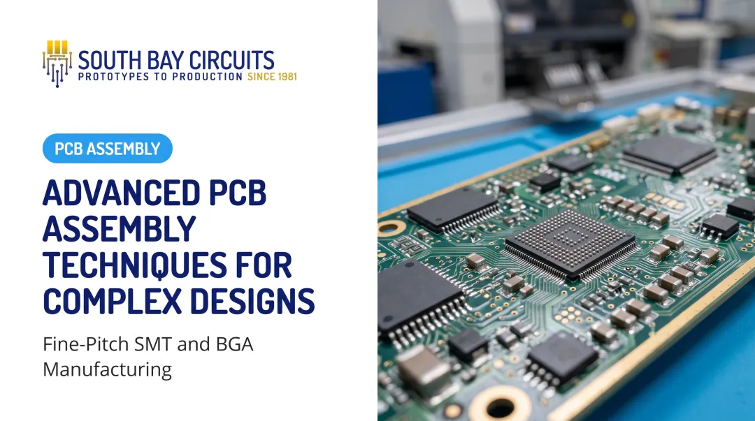
SMT mounts components directly onto the board surface, with leads or terminals soldered to pads using a reflow process. THT inserts leaded components through drilled holes, secured on the opposite side using wave or selective soldering.
Neither method has fully replaced the other: SMT dominates modern designs because it supports higher component density and smaller footprints, while THT persists for connectors, transformers, and parts that need extra mechanical strength to survive repeated plugging or physical stress.
Most production boards today use a mixed-technology approach. SMT handles the dense digital circuitry, while THT covers the parts that take a physical beating in the field.
Why PCB Assembly and Soldering Matter in Electronics Manufacturing
A solder joint is the only thing standing between a working device and a failed one when that device gets dropped, vibrated, heated, or exposed to humidity. Reliable soldering is what lets electronics function consistently outside a lab environment.
Demanding industries expect three things from their assembly partner: consistency, tight tolerances, and full traceability. That's non-negotiable in sectors like:
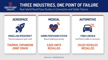
- Aerospace, where a cracked joint discovered during Magellan spacecraft integration testing was traced back to thermal expansion mismatches in the assembly, not the solder alloy itself
- Medical devices, where the FDA issued a Class 2 recall covering 3,022 units of the Sarns Modular Perfusion System after monitor-board soldering anomalies caused intermittent pressure display and pump-stop issues
- Automotive, where Ford's 2025 recall affected 213,121 Lincoln Aviator and Ford Explorer vehicles due to insufficient solder at a body control module connector, a defect that could disable trailer taillamps
Without disciplined process control, common defects creep in:
- Cold joints (insufficient heat, leaving a weak bond)
- Tombstoning (a component standing on one end after reflow)
- Solder bridging (unintended connections between adjacent pads)
- Component misalignment from placement or paste volume errors
These aren't cosmetic flaws. They cause intermittent field failures or outright board rejection.
That's the reason the industry runs on formal standards. IPC-A-610 sets the acceptability criteria for solder joints and electronic assemblies. On top of that, compliance-driven sectors layer their own quality system requirements: AS9100 for aerospace, ISO 13485 for medical, and ISO/TS 16949 for automotive.
South Bay Circuits holds certifications across ISO 13485, ISO/TS 16949, and AS9100 compliance, alongside ISO 9001:2015. That combination exists specifically to serve OEMs who need cross-industry reliability standards met under a single roof, rather than chasing down separate certifications from separate vendors.
How PCB Assembly and Soldering Works (Step-by-Step)
At a high level, the process runs from design verification through component placement and soldering, ending in inspection and testing. Every joint has to meet a documented specification before the board ships.
Inputs required before production starts:
- A verified bill of materials (BOM)
- Gerber or ODB++ design files
- Solder paste matched to the assembly's thermal profile
- The physical components themselves, sourced and verified
Solder paste (or molten solder, for THT) is heated past its melting point. As it cools, it forms a metallurgical bond between the component lead and the copper pad. Everything else in the workflow exists to control that transformation and catch defects before they reach a customer.
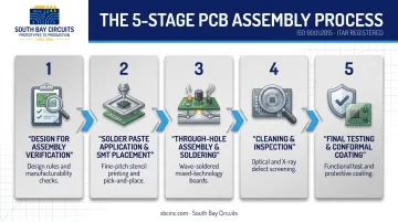
Step 1: Design for Assembly (DFA) Verification
Before anything gets built, engineers review the BOM, Gerber files, and component footprints for spacing, orientation, and thermal relief problems. Catching a footprint error here costs minutes. Catching it after reflow costs a rebuilt board.
Step 2: Solder Paste Application and SMT Component Placement
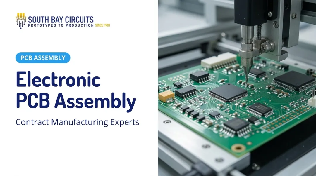
Solder paste gets applied through a stencil onto exposed pads. A pick-and-place machine then mounts SMT components onto that paste before the board travels through a reflow oven.
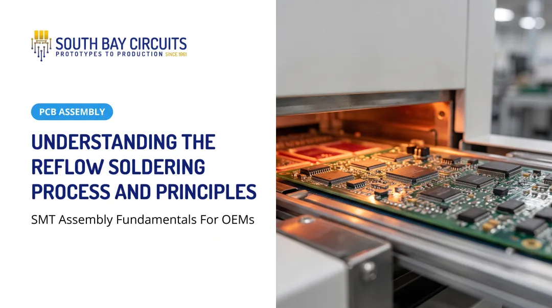
Reflow temperature profiles are paste-specific rather than universal. As a reference point, Kester's 909HPS lead-free paste calls for a peak temperature of 235-250°C, while AIM's WS483 SAC305 paste specifies 230-245°C. Both datasheets stress that the exact profile depends on oven type and board layout, so treat these as starting benchmarks, not fixed rules.
Step 3: Through-Hole Assembly and Soldering
THT components get inserted into drilled holes, then secured using one of three methods depending on volume and part sensitivity:
- Wave soldering for high-volume runs
- Selective soldering for boards with heat-sensitive SMT parts nearby
- Hand soldering for low-volume or highly complex boards
Step 4: Cleaning and Inspection
Once soldering is complete, boards get cleaned of flux residue. Inspection follows using AOI (automated optical inspection), X-ray for hidden joints like BGAs, and flying probe testing to catch missing components, bridging, or weak connections before they become field failures.
Step 5: Final Testing and Conformal Coating
Completed boards go through functional testing to confirm they perform as designed. For products headed into harsh environments (moisture, dust, vibration), a protective conformal coating gets applied before shipment.
Key Factors That Affect Assembly and Soldering Quality
Several variables determine whether a joint meets spec or ends up in the rework pile:
- Component and material quality – Reliable sourcing prevents counterfeit or out-of-spec parts that compromise joint integrity
- Temperature control – An off-target reflow or wave profile causes cold joints, tombstoning, or outright component damage
- Equipment precision – Pick-and-place accuracy and stencil design directly affect paste deposition and placement alignment
- Board complexity and volume – Dense, fine-pitch designs or high-mix, low-volume runs demand different soldering approaches than simple, high-volume boards
- Regulatory requirements – Aerospace and medical customers often mandate specific IPC classes, plus full documentation traceability
IPC guidance doesn't automatically assign every aerospace or medical board to Class 3. The customer specifies the required class in the contract or purchase order. Assuming a higher class than what's contracted, or a lower one, creates problems either way.
South Bay Circuits builds to whatever IPC class a contract calls for, including Class 3 for aerospace, defense, and medical programs, with documentation and traceability matched to the customer's exact specification.
Common Mistakes and Choosing the Right Assembly Partner
Common Mistakes That Undermine Assembly Reliability
Hand soldering and automated soldering aren't interchangeable. Volume and component sensitivity should dictate the method, not convenience. A single-unit prototype doesn't need a wave soldering line, and a 50,000-unit production run has no business relying on hand soldering.
"No-clean flux" doesn't mean no cleaning is required. Properly activated no-clean residue can perform fine in many applications.
But trapped, hygroscopic residue combined with moisture and electrical bias can support electrochemical migration over time. Ion chromatography and surface-insulation-resistance testing are the accepted ways to validate residue behavior for a given environment, rather than just assuming it's safe.
Joint appearance alone doesn't confirm reliability. A shiny joint isn't always sound, and a dull one isn't always defective. Dull, lumpy, or granular joints are a common signal of cold solder connections, though, and they warrant a closer look and possible rework.
Full automation isn't always the right call. Very low-volume prototypes, or boards that go through frequent last-minute design changes, are often better served by selective or hand soldering than by setting up an automated line for a handful of units.
What to Look for in an Assembly Partner
Avoiding these mistakes starts with vetting the partner responsible for execution. When evaluating a partner, ask for:
- Documented IPC class and revision requirements
- Paste-specific thermal profiles, not generic templates
- Qualified wave, selective, and hand soldering procedures
- AOI, X-ray, and electrical test coverage appropriate to the board
- Residue validation data, not just assurances
This is where a single-source model changes the equation. South Bay Circuits handles PCB design, fabrication, and assembly from one 60,000 square foot facility in Chandler, Arizona, with in-house SMT lines and quick-turn scheduling from same-day to standard production runs.
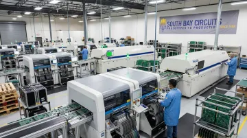
When design, fabrication, and assembly sit under one roof, there's no vendor-to-vendor blame game when something goes wrong. Just one accountable process from layout to loaded board.
Frequently Asked Questions
What is PCB assembly and soldering?
PCB assembly is the process of populating a bare circuit board with electronic components. Soldering is the specific technique used within that process to permanently bond those components electrically and mechanically to the board.
Does soldering damage a PCB?
Properly controlled soldering does not damage a PCB. However, excessive heat, poor temperature profiling, or repeated rework cycles can cause pad lifting, delamination, or component damage over time.
What's the difference between wave soldering and reflow soldering?
Wave soldering passes through-hole components over a molten solder wave to form connections. Reflow soldering melts pre-applied solder paste in an oven, primarily for surface mount components.
Can SMT and through-hole components be assembled on the same PCB?
Yes, mixed-technology assembly is standard practice. SMT components are typically reflow soldered first, followed by through-hole components added via wave, selective, or hand soldering.
How can you tell if a solder joint is bad?
Bad joints often look dull, cracked, or lumpy rather than smooth and consistent. This appearance can indicate insufficient heat, contamination, or an unreflowed particle during the soldering process.
What IPC standard governs PCB solder joint quality?
IPC-A-610 is the primary industry standard defining acceptability criteria for solder joints and electronic assemblies. It defines visual acceptability criteria only, so the manufacturing process used to achieve those results still requires separate qualification.