Introduction
ICT testing, short for in-circuit testing, is an automated electrical test method that checks individual components and connections on a populated PCB for manufacturing defects.
If you buy or engineer PCB assemblies for medical devices, aerospace systems, automotive electronics, or industrial equipment, you've likely seen ICT referenced in an RFQ or spec sheet without much explanation.
That's a problem. Catching a defect at the component level, before the board moves further down the line, matters directly for quality, regulatory compliance, and long-term reliability. Yet ICT remains one of the most cited but least understood terms in electronics manufacturing conversations.
This article breaks down what ICT actually is, why manufacturers rely on it, how the process works step-by-step, where it fits in a production line, and the specific situations where it isn't the right call.
Key Takeaways
- Catches shorts, opens, and wrong or missing components by probing predefined test points on the assembled board
- Delivers the speed and pin-level fault location that make it the standard for high-volume production
- Requires a custom bed-of-nails fixture and DFT-focused PCB design, so ROI favors production-scale volumes
- Works best layered with AOI, X-ray, flying probe, or functional testing—not as a standalone screen
What Is ICT Testing?
In-circuit testing verifies the electrical integrity and component values on an assembled PCB. A fixture or a set of flying probes makes physical contact with designated test points, sending and reading electrical signals to confirm the board was built correctly.
The goal is straightforward: catch manufacturing and assembly defects at the component level before the board advances to the next stage. A short circuit, an open connection, or a wrong-value resistor caught here costs far less to fix than the same defect discovered during functional test or, worse, in the field.
ICT vs. FCT (Functional Circuit Test)
These two methods answer different questions, and confusing them is one of the most common mistakes buyers make.
- ICT checks structure and components largely in isolation — did the right parts get placed correctly, and are the connections intact?
- FCT powers up the finished board and validates that it actually performs its intended real-world function, such as communicating over an interface or executing firmware correctly.
Keysight's own white paper on the topic frames these as complementary rather than interchangeable: ICT catches structural defects early, while FCT validates finished-product behavior near the end of manufacturing. You generally need both for a complete quality picture.
ICT vs. Flying Probe Testing
The other frequent point of confusion is fixture-based ICT versus flying probe testing:
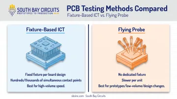
- Fixture-based ICT uses a fixed bed-of-nails fixture built for one board design, contacting hundreds or thousands of points at once for speed at volume.
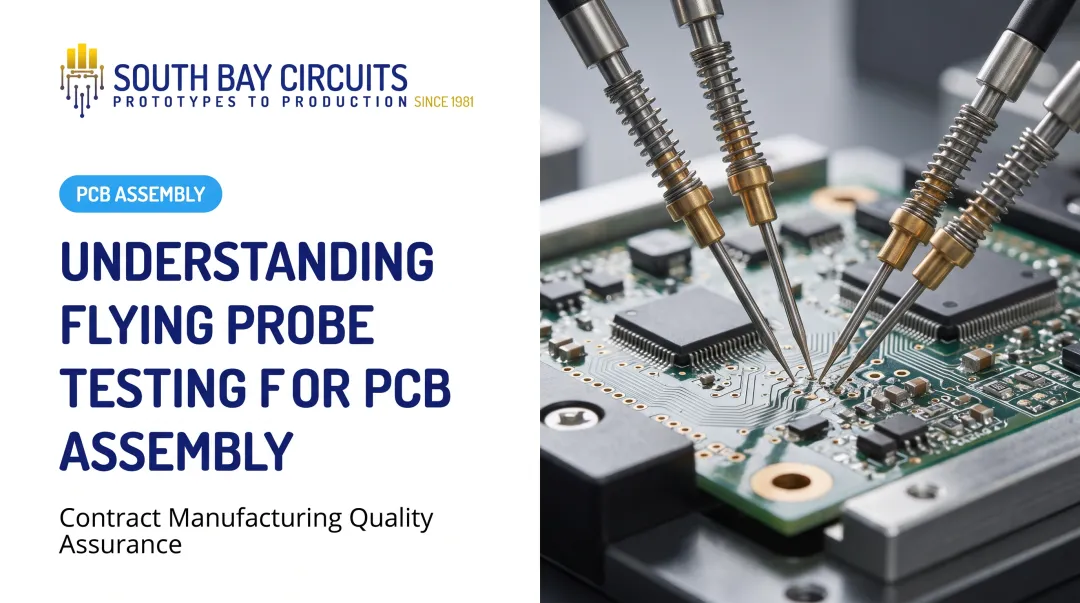
- Flying probe uses moving probes with no dedicated fixture, so it is slower per unit but better suited to prototypes, design changes, or low-volume runs.
Core Equipment Involved
A typical ICT setup includes:
- A test head that houses the measurement electronics
- An interface or fixture board holding the bed-of-nails pins
- Control software that sequences tests and compares results
- A power supply for powered test stages
- Spring-loaded probe pins that physically contact test points
South Bay Circuits, for example, runs a Teradyne Z1860VP ICT system with 2,048 test points and wave-scan/delta-scan capability. The line uses bed-of-nails fixtures for single-sided boards and clam-shell fixtures for double-sided SMT assemblies.
Why ICT Testing Is Used in Manufacturing
High-volume, high-mix electronics manufacturing demands consistency across thousands of units, full traceability, low defect escape rates, and fast per-unit testing. ICT addresses all four simultaneously: it's automated, repeatable, and can isolate a fault to a specific component in seconds rather than minutes.
The Cost of Catching Defects Late
Defects don't get cheaper to fix the longer they sit undetected. Research published by IEEE on PCB assembly test processes confirms this directly: earlier detection of process and electrical defects lowers the total cost of ownership across the manufacturing lifecycle.
A short or open that slips past ICT and reaches functional test, or worse, the field, triggers more diagnostic time, more rework labor, and in regulated industries, potential compliance documentation gaps.
Regulatory and Quality Drivers
Manufacturers serving regulated sectors typically hold certifications such as:
- ISO 9001:2015 — general quality management systems
- AS9100 — aerospace and defense
- ISO 13485 — medical devices
- IATF 16949 — automotive
None of these standards names ICT specifically as a requirement. What they do require is documented, repeatable process verification and objective evidence of quality control.
ICT is one of the most reliable ways to generate that evidence at the component level, which is why manufacturers in these sectors rely on it heavily, even without an explicit line-item mandate.
South Bay Circuits holds ISO 9001:2015 certification (certificate 10000903 QM15) and maintains ISO 13485, AS9100, and IATF 16949 compliance. That documented verification supports customers in medical, aerospace, automotive, and industrial programs.
In practice, ICT is often a customer expectation in high-reliability sectors, where a single undetected defect can mean a recall or field failure.
How ICT Testing Works (Conceptual Flow)
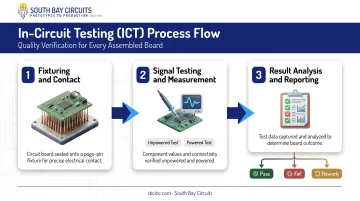
The process is straightforward. The PCBA sits in a test fixture, probes contact designated test points, and the tester sends and reads electrical signals. It then compares those results against stored specifications.
Building that test requires three inputs:
- The assembled board itself
- A test program built from CAD and schematic data
- Predefined pass/fail specifications for every tested node
Step 1: Fixturing and Contact
The board loads into a custom bed-of-nails fixture, or a flying-probe system contacts it when no fixture exists. Spring-loaded pins align with test points etched into the board layout during design. Poor alignment here means poor test coverage later, regardless of how strong the test program is.
Step 2: Signal Testing and Measurement
Before anything else, the tester discharges capacitors as a safety and accuracy step, protecting both the board and its sensitive circuitry. From there, it runs a structured sequence:
- Unpowered tests — continuity, resistance, capacitance checks against opens and shorts
- Powered tests — digital logic verification, analog behavior, and device programming where applicable
Guarding and switching circuits isolate individual components during measurement so signals don't bleed across the board and produce false readings. Built-in self-diagnostics confirm the tester itself is working correctly before any results are accepted.
Step 3: Result Analysis and Reporting
The system compares every measurement against stored tolerances, flags discrepancies, and marks the board one of three ways:
- Pass — moves to the next production stage
- Fail — scrapped or held for rejection
- Rework — returned for repair and retest
It also generates a test report for quality records. In mature operations, this data feeds an ERP or MES system for traceability and process improvement, helping engineers spot recurring defect patterns early.
Where ICT Fits and What Affects Its Performance
ICT typically runs after SMT assembly and reflow, but before functional or system-level testing. It acts as an early checkpoint, catching structural defects before the board reaches more expensive, time-consuming test stages. Unlike spot-check methods, ICT runs inline for every unit in high-volume production.
Several factors determine how much of the board ICT can actually reach and verify:
- PCB design for testability: accessible test pads, tooling holes, and adequate spacing directly determine achievable coverage
- Board complexity and density: fine-pitch parts and BGAs can physically block probe access to certain nodes
- Fixture and probe wear: repeated high-volume contact degrades pins over time, requiring ongoing maintenance to preserve accuracy
- Production volume and lifecycle: determines whether the upfront fixture investment pays off
- Industry-specific requirements: aerospace and medical programs may dictate minimum acceptable test coverage thresholds
Keysight's engineering guidance on this point is blunt: conventional 100% test access is often no longer achievable on modern, densely populated boards. That's why DFT review matters before layout is finalized, not after. South Bay Circuits builds DFM/DFT verification into its standard layout process, working with customers from early design through production to flag testability concerns before they become fixture-stage problems.
Common Misconceptions and When ICT May Not Be the Right Fit
"High Coverage Means Zero Defects"
Not quite. Coverage percentages measure how many known defect types a test can catch within a specific dataset, not how many nets are physically probed or every possible fault.
An IPC-hosted industry study analyzing nine manufacturing sites found ICT test effectiveness averaged 26.1%, with individual site results ranging from 20% to 60% depending on the defect set tested. That's a meaningful gap between "tested" and "guaranteed defect-free."
"ICT Alone Proves the Board Works"
ICT validates structure and components. It doesn't confirm real-world operational behavior; that's FCT's job. A board can pass every ICT node and still fail to perform its intended function if the firmware is wrong or a design flaw exists that ICT wasn't built to catch.
When ICT Isn't Worth It
ICT generally isn't cost-effective for:
- Low-volume runs: the custom fixture cost is hard to amortize across a small unit count
- Short product lifecycles: by the time the fixture pays for itself, the product may be obsolete
- Extremely dense or miniaturized boards: physical probe access may simply not exist without redesigning the layout
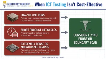
In these cases, flying probe testing or boundary scan often makes more sense. The right choice depends on volume, design maturity, and lifecycle needs, not default habit.
An experienced single-source manufacturer like South Bay Circuits, which runs both ICT and flying probe systems in-house, can help evaluate which approach (or combination) fits a specific project's design-for-test requirements and production volume.
Frequently Asked Questions
What is ICT and FCT testing?
ICT checks individual component values and connections on an unpowered or partially powered board. FCT fully powers the board to verify it performs its intended real-world function.
How is an ICT test done?
The board loads into a fixture, probes contact test points, and the tester runs unpowered and powered measurement sequences. The system compares results against stored pass/fail specifications.
What is the difference between ICT and flying probe testing?
ICT uses a fixed bed-of-nails fixture suited to high-volume speed. Flying probe testing uses moving probes with no fixture, making it better suited to low-volume or prototype work.
What defects can ICT testing detect?
ICT catches shorts, opens, wrong, missing, or misoriented components, incorrect component values, and basic functional faults such as faulty digital logic.
Is ICT testing cost-effective for low-volume production runs?
Usually not. The upfront fixture cost is difficult to amortize at low volumes, so flying probe testing typically makes more economic sense for smaller runs.
Why is Design for Testability (DFT) important for ICT?
Without probe-able test pads and proper spacing built into the PCB layout, achievable ICT coverage drops significantly, regardless of how capable the tester itself is.