For engineers, product designers, procurement managers, and OEM teams in aerospace, medical, defense, and industrial sectors, understanding PCBA at an operational level — not just a definitional one — directly affects quality, cost, and time-to-market. A board that fails final inspection or arrives with documentation-driven delays costs far more than the assembly itself.
This guide covers what PCBA means, how it differs from a bare PCB, how the process works from DFA review through final inspection, and where common misunderstandings create expensive problems.
Key Takeaways
- A PCB is a bare, non-functional substrate; PCBA is the populated, soldered, tested board ready for integration
- SMT and through-hole technology are the two primary assembly methods — most modern boards use both
- Assembly follows a fixed sequence: DFA review, solder paste, component placement, reflow, through-hole, cleaning, then inspection
- Documentation accuracy and component sourcing integrity determine outcomes before a single component is placed
- Selecting the wrong assembly partner or underestimating process complexity is a leading driver of costly production failures
What Is Printed Circuit Board Assembly (PCBA)?
PCBA is the result of mounting, placing, and soldering electronic components — resistors, capacitors, ICs, connectors, and more — onto a fabricated PCB. The outcome is a board that can power on, carry electrical signals, perform its designed circuit function, and integrate into an end product or system.
PCB vs. PCBA: Not the Same Thing
These two terms get used interchangeably, but they describe fundamentally different things.
| PCB | PCBA | |
|---|---|---|
| What it is | Bare fabricated board | Populated, soldered board |
| Contains components? | No | Yes |
| Functional? | No | Yes |
| Ready for integration? | No | Yes |
The PCB has etched copper traces, drilled holes, and solder mask applied — but it performs no electronic function on its own. The PCBA is the completed assembly, ready for use.
The Two Primary Assembly Technologies
Two core methods define how components are attached to a PCB:
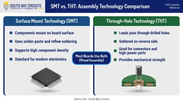
- Surface Mount Technology (SMT): Components mount directly onto the board surface using solder paste and reflow soldering. SMT supports high component density and is the standard method in modern electronics manufacturing.
- Through-Hole Technology (THT): Component leads pass through drilled holes and are soldered on the opposite side. Used for connectors, high-power components, and parts requiring mechanical strength.
Most production boards use a mixed assembly approach — SMT on the primary side, through-hole for specific components where the application demands it.
Where PCBA Fits in the Product Lifecycle
Understanding the assembly technologies helps clarify where PCBA sits in the broader process: after PCB fabrication and before final integration or box build. Before assembly can begin, a complete documentation package is required — BOM, Gerber or ODB++ files, assembly drawing, and pick-and-place file. Incomplete or inaccurate documentation at this stage introduces delays that carry through every subsequent step.
How the PCBA Process Works, Step by Step
PCBA follows a controlled, sequential process where each stage builds on the last. Errors introduced early — in documentation, component sourcing, or paste application — propagate through all subsequent steps and increase the cost of correction at every stage.
Step 1: Design for Assembly (DFA) Review
Before any physical assembly begins, DFA engineers verify the Gerber or ODB++ files and BOM for accuracy. The IPC checklist for producing rigid printed board assemblies specifies review of component footprints, land patterns per IPC-7351, pad spacing, board edge clearances, drill specifications, and thermal relief requirements — including BGA/CSP per IPC-7095 and QFN per IPC-7093.
Catching design errors here costs far less than correcting them after placement.
Step 2: Solder Paste Application
Solder paste (a mixture of powdered metal solder and flux) is applied to SMT pads using a stainless steel stencil, which deposits precise volumes of paste at each pad location. Stencil design follows IPC-7525.
After printing, 2D or 3D solder paste inspection (SPI) machines verify paste volume, width, and coverage before component placement proceeds. A skipped or abbreviated SPI step allows paste defects (bridging, insufficient coverage, slump) to carry through to reflow.
Step 3: SMT Component Placement
Automated pick-and-place machines retrieve components from reels or trays, orient them to the correct rotation, and place them onto the solder paste deposits. This step requires an accurate centroid or pick-and-place file defining component location, rotation, and placement side.
South Bay Circuits operates Fuji SMT lines, including CP-642 and CP-65 chipshooters and the IP-3 flexible placer with tray tower, capable of handling components down to 0201 packages, fine pitches to 0.3mm, BGAs, CSPs, and quad-flat packs.
Step 4: Reflow Soldering
The board passes through a reflow oven, where controlled temperature zones heat the solder paste to its liquidus point and allow it to cool and solidify, forming permanent electrical and mechanical connections. Temperature profiles are calibrated to the solder paste specification (per J-STD-005) and the board's thermal requirements. Off-profile reflow causes cold joints, bridging, or component damage.
Step 5: Through-Hole Component Assembly
Components with leads that pass through drilled holes — connectors, large capacitors, transformers — are assembled after SMT. Three soldering methods apply:
- Wave soldering — for large batches of through-hole components
- Selective soldering — for specific through-hole locations on a mixed-technology board
- Hand soldering — for sensitive or low-volume components
The appropriate method should be specified in the assembly notes. Leaving this decision to the assembler without guidance increases the risk of selecting a method that doesn't match the thermal or mechanical requirements of the component.
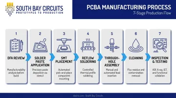
Step 6: Cleaning
After soldering, boards are cleaned with deionized water or chemical solutions to remove flux residue and ionic contaminants that cause corrosion or electrical leakage over time. IPC-CH-65 is the IPC cleaning guideline; IPC-A-610J Section 10.6 addresses cleanliness and residues on completed assemblies.
Non-washable components — those sensitive to moisture or cleaning chemistry — are masked before washing and soldered separately using no-clean flux after the cleaning step. This must be specified in the assembly notes. Omitting it leads to component damage or incorrect flux selection.
Step 7: Inspection and Testing
Once cleaning is complete, inspection verifies the assembly meets acceptability criteria before delivery. Multiple methods are applied, each examining different attributes:
| Method | What It Detects |
|---|---|
| AOI (Automated Optical Inspection) | Missing components, misalignments, solder bridges, insufficient solder |
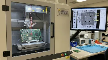
| X-ray inspection | Hidden solder joints — BGAs, QFNs, CSPs |
| Flying Probe Testing (FPT) | Continuity, opens, shorts, component values |
| Functional testing | Confirms the board operates as designed |
At South Bay Circuits, all BGA placements are verified by X-ray inspection on every assembly produced — not as an optional step. IPC-A-610J (Revision J, published March 2024) defines the acceptability criteria for solder joints, component placement, and cleanliness across all inspection categories.
Conformal coating may also be applied as a final step for boards destined for harsh environments — high humidity, temperature cycling, or chemical exposure.
Key Factors That Affect PCBA Quality and Outcomes
Quality in PCBA is determined before the first component is placed. These are the factors that matter most:
Documentation completeness and accuracy An incomplete BOM, incorrect Gerber files, or missing assembly notes are the most common root causes of manufacturing delays and misbuilds. The IPC assembly checklist requires a complete BOM, component data, schematic, placement data, and defined performance class before assembly can begin.
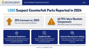
Component sourcing and supply chain integrity ERAI's 2024 annual report recorded 1,055 suspect counterfeit and nonconforming parts — 25% above 2023 levels. Obsolete components represented 42.75% of reports. Components procured from unverified sources introduce the risk of counterfeit, incorrect specification, or date code failures. Sourcing through authorized distributors or working with a contract manufacturer that has established component management practices directly reduces this exposure.
Process control and equipment capability Solder paste volume, reflow oven temperature profile accuracy, pick-and-place placement precision, and cleaning process parameters all have direct effects on solder joint integrity and long-term board reliability. Without calibrated equipment and documented process controls, even a well-designed board will produce inconsistent solder joints and field failures.
Single-source vs. multi-vendor workflow When PCB fabrication and assembly are handled by separate vendors, queue times, shipping, and communication gaps between the fab and assembly house add lead time and reduce process visibility. A single-source provider managing both fabrication and assembly under one roof eliminates these handoff delays and maintains complete process accountability from bare board through populated assembly. South Bay Circuits operates this way from its 60,000 sq ft Chandler, AZ facility, with 3-Day Turn or Less assembly capability available for qualifying builds..
Scale, volume, and design stability Prototype builds require flexibility and frequent design iteration. Production runs benefit from optimized, stable processes. The assembly approach, tooling, and inspection investment should match the volume and design maturity of the program.
Where and Why PCBA Is Applied
PCBA spans every sector where electronics matter — and the quality, compliance, and documentation requirements vary considerably across them.
Industries and Applications
- Aerospace and defense — avionics, guidance systems, communications hardware; AS9100D quality management requirements apply
- Medical devices — imaging systems, patient monitoring, implantables; ISO 13485:2016 governs QMS requirements
- Automotive electronics — engine management, ADAS, infotainment; IATF 16949:2016 applies
- Industrial controls — automation, power conversion, instrumentation
- Consumer electronics — highest volume, lower documentation intensity
Lifecycle Stages
The assembly process is consistent across lifecycle stages, but the level of inspection, documentation, and qualification testing increases as programs mature:
- Prototype and NPI builds — low volume, high change frequency, emphasis on DFA feedback and design flexibility
- Pre-production validation — first-article inspection, process qualification, documentation lock
- Full production runs — optimized, stable processes with ongoing process control and statistical monitoring
Regulated industries require PCBA providers to hold specific quality management certifications and maintain traceability records throughout every stage. South Bay Circuits carries ISO 9001:2015, AS9100, ISO 13485, ITAR registration, and CMMC Level 1 compliance — meaning customers in aerospace, medical, and defense can qualify a single source for both fabrication and assembly rather than managing separate vendor relationships.
That compliance footprint matters at scale. According to Grand View Research, the global PCBA market was valued at $98.9 billion in 2025 and is projected to reach $137.4 billion by 2033 at a 4.3% CAGR — a figure that reflects just how much of the electronics supply chain depends on consistent, well-documented assembly quality.
Common Misconceptions and Pitfalls in PCBA
"Assembly Is Just an Automated Extension of Fabrication"
This is the most common and costly misunderstanding. PCBA requires its own complete documentation package, DFA review, process engineering, and quality oversight — none of which fabrication automatically provides.
Treating it as a commodity handoff — sending a BOM and Gerber files without assembly notes, IPC class designation, or washability callouts — generates engineering queries, delays, and assembly errors that rework rarely fully recovers from.
"SMT Is Always the Right Choice"
SMT is not universally superior to through-hole. Some components are only available in through-hole packages — high-power devices, large connectors, certain sensors — or require the mechanical strength of a through-hole joint that solder paste reflow cannot replicate. Selecting SMT by default when THT is more appropriate creates reliability risks, particularly in high-vibration or high-current applications.
Common Process Pitfalls to Avoid
Beyond conceptual errors, operational shortcuts introduce their own failure modes:
- Skip or abbreviate the DFA review and the time "saved" typically comes back as rework, scrap, or production delays
- Submit a BOM without an Approved Vendor List (AVL) and you open the door to component substitutions that may not meet specification
- Omitting assembly notes on washable vs. non-washable components leads to component damage during cleaning
- First-article inspection (FAI) is a point-in-time quality gate — not a perpetual sign-off; any process or component change requires revisiting it
Frequently Asked Questions
What is the difference between PCB and PCB assembly?
A PCB (printed circuit board) is a bare, unpopulated board with etched copper traces — it has no electronic function on its own. PCB assembly (PCBA) is the completed board after components have been placed and soldered onto it, making it functional and ready for integration into an electronic product.
What is the main purpose of a PCB?
A PCB mechanically supports and electrically connects electronic components through a network of conductive copper traces etched into a non-conductive substrate. It replaces point-to-point wiring and enables compact, repeatable, automated manufacturing of electronic circuits.
What does "printed circuit" mean?
A printed circuit refers to the pattern of electrical conductors — traces, pads, and vias — etched or deposited onto an insulating substrate using photolithographic processes. The term "printed" reflects how that circuit pattern is transferred onto the board material.
What are the two main methods used in PCB assembly?
Surface Mount Technology (SMT) places and solders components directly onto the board surface. Through-Hole Technology (THT) passes component leads through drilled holes and solders them on the reverse side. Most modern boards use both methods in a mixed assembly approach.
How long does PCB assembly typically take?
Lead time depends on board complexity, component availability, volume, and the assembly provider's capabilities. Prototype builds can be completed in hours; standard production runs typically take days to weeks.
What quality standards apply to printed circuit board assembly?
IPC-A-610 (Revision J, March 2024) is the primary workmanship standard, covering solder joint acceptability, placement, and cleanliness. Industry-specific standards include AS9100D for aerospace, ISO 13485:2016 for medical devices, and IATF 16949:2016 for automotive electronics.