That shortage is pushing more companies to outsource PCB design and layout instead of building an internal team from scratch. Common pain points driving this shift include:
- Limited in-house engineering bandwidth for complex boards
- Rising NPI (New Product Introduction) costs tied to redesigns and missed deadlines
- The risk of picking the wrong outsourcing partner and paying for it later
This guide breaks down what outsourcing actually involves, its real benefits and cost drivers, how to vet a partner, the mistakes to avoid, and how a single-source manufacturer like South Bay Circuits simplifies the entire process.
Key Takeaways
- Outsourcing frees engineering bandwidth without a full-time senior design hire
- Costs scale with layer count, board technology, design scope, and certification requirements
- Single-source, design-to-assembly partners cut hand-off delays and shorten NPI timelines
- AS9100, ISO 13485, and IATF 16949 certifications matter as much as price when vetting a partner
- The cheapest quote often hides costs in rework, scrap, and missed deadlines
What Is PCB Design and Layout Outsourcing?
"PCB design" and "PCB layout" get used interchangeably, but they're two distinct disciplines.
PCB design covers schematic capture: the engineer defines circuit connectivity, selects components, and establishes design intent before anything touches a board outline.
PCB layout picks up from there, covering board shape and layer-stack definition, component placement, copper routing, and the design-rule checks that feed into DFM (design for manufacturability) and DFT (design for testability) analysis.
"Outsourcing" can mean handing off just one of these stages or both. Some companies keep schematic capture in-house and send out only the physical layout. Others hand off the entire process from concept to final files.
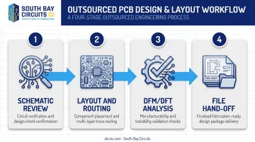
A typical outsourced workflow looks like this:
- Schematic review - the partner audits your circuit design for completeness and manufacturability red flags
- Layout and routing - component placement, layer stack-up, and copper routing based on your design rules
- DFM/DFT analysis - checking the layout against fabrication and test capabilities before release
- File hand-off - delivering Gerber, ODB++, and BOM data to fabrication
Companies typically send this work to one of three types of providers:
- Independent freelance designers
- Specialized PCB design houses focused exclusively on layout
- Full-service contract manufacturers that also fabricate and assemble the board in-house
That last option removes an entire hand-off point from the process.
Key Benefits of Outsourcing PCB Design and Layout
Outsourcing isn't just about offloading work you don't have time for. Done well, it changes the economics and the risk profile of the entire project.
Cost Efficiency
Building an in-house PCB design team means paying for senior engineer salaries, EDA software licenses, and ongoing training. The median annual wage for electronics engineers was $127,590 in May 2024, and that figure doesn't include benefits, payroll taxes, recruiting, or software licensing (Bureau of Labor Statistics).
Outsourcing turns that fixed overhead into a variable, per-project cost.
Access to Specialized Expertise
Most in-house teams handle general-purpose boards well but struggle with HDI, rigid-flex, or high-speed signal integrity work. Outsourced partners bring engineers who work on these formats daily:
- High-density interconnect (HDI) and advanced packaging
- Rigid-flex mechanical and electrical design
- RF/microwave and high-speed digital signal integrity
- DFM-focused design reviews
Faster Time-to-Market
Dedicated layout teams, without other engineering responsibilities pulling their attention, generally turn projects around faster than an internal engineer splitting time across five priorities. That speed can compress your NPI cycle.
But it's not automatic. One EE Times study found average product-design time actually rose 20% at OEMs as outsourcing expanded, largely due to coordination overhead between separate vendors (EE Times). The speed benefit depends heavily on how well-coordinated the relationship is.
Improved Design for Manufacturability (DFM)
Experienced partners catch manufacturability issues, like insufficient trace clearances or unrealistic via sizes, before the board reaches fabrication. Catching these problems early prevents:
- Costly re-spins after the first prototype run
- Scrap from boards that can't be reliably fabricated
- Yield loss during assembly caused by tight tolerances
Single-Source Advantage
Using one partner for design, fabrication, and assembly eliminates the hand-offs where files get lost, formats don't match, or two vendors point fingers over a delay.
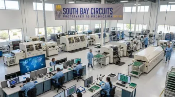
This is where South Bay Circuits' model fits. Design, layout, fabrication, assembly, and box builds all happen inside the same 60,000-square-foot Chandler, Arizona facility. There's no queue time between processes, and no ambiguity about who owns a manufacturability issue.
Factors That Influence the Cost of Outsourcing PCB Design and Layout
Quotes for the same-sounding project can vary wildly. Here's what actually drives the number.
Circuit Complexity and Layer Count
More layers mean more design hours. A simple 2-layer board might take a few hours to route; a 6+ layer board with tight component density and controlled impedance requirements can take days. Layer count and routing density are the biggest cost drivers in most quotes.
Board Type and Technology
Standard rigid boards command standard rates. Specialized formats require niche expertise and carry a premium:
- HDI boards with microvias and sequential lamination
- Rigid-flex boards combining flexible and rigid substrates
- RF/microwave boards requiring controlled impedance and shielding
Design Scope
Pricing depends on exactly what you're asking for:
- Layout and routing only from a completed schematic
- Full schematic-to-production support, including component selection and DFM/DFT analysis
- Ongoing support across multiple product revisions
Layout-only work costs less per board but assumes your schematic is already solid.
Certification and Industry Requirements
Boards headed for aerospace, medical, or automotive applications need added engineering rigor:
- AS9100 requires controlled documentation for processes affecting product conformity, even outsourced ones
- ISO 13485 applies similar rigor to medical-device design, emphasizing risk-based controls and supplier oversight
- IATF 16949 requires automotive suppliers to document how outsourced processes are identified and controlled
All three add engineering and documentation overhead that shows up in the price.
Onshore vs. Offshore Providers
Offshore design houses typically quote lower hourly rates than domestic full-service partners, but the trade-offs are real:
| Factor | Offshore | Onshore |
|---|---|---|
| Hourly rate | Generally lower | Generally higher |
| Communication speed | Slower, time zone gaps | Faster, same-day turnaround |
| IP protection | Varies by country's laws | Easier to enforce under US law |
| Compliance verification | Harder to audit | Easier to audit against US standards |
For boards with tight compliance requirements or sensitive IP, a lower offshore rate can end up costing more once rework and delays are factored in.
How to Choose the Right PCB Design and Layout Outsourcing Partner
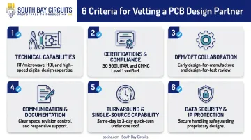
Vetting a partner properly upfront saves you from expensive surprises mid-project. Focus on these six areas before signing a contract:
Technical capabilities and equipment: Verify the partner has actually worked on your specific board type, not just claims to. Ask for examples of HDI, rigid-flex, or multilayer projects similar to yours, and confirm they use modern EDA tools with built-in DFM checking.
Certifications and compliance: ISO 9001 should be table stakes. For regulated industries, match the certification to your application: AS9100 for aerospace, ISO 13485 for medical devices, IATF 16949 for automotive. South Bay Circuits holds all three, plus ITAR registration and CMMC Level 1 compliance for defense-related work.
DFM/DFT collaboration: Bring your partner's engineers into the design phase early, not after the layout is finished. Early collaboration catches manufacturability and testability problems while they're still cheap to fix.
Communication and documentation standards: A partner needs clean processes for managing Gerber files, BOMs, and revision control. Ask upfront how they track file versions and what documentation package they expect from you before work begins.
Turnaround time and single-source capability: Ask whether the provider can take your design straight from layout into fabrication and assembly without shipping files to a third party. Every hand-off between separate vendors adds queue time and risk of miscommunication.
Data security and IP protection: Before sharing proprietary design files, confirm the partner has:
- A signed NDA or confidentiality agreement
- Secure file transfer protocols
- Access controls limiting who can view your data
This matters even more for defense and medical designs, where technical data may fall under export control or privacy regulations.
Common Risks and Mistakes to Avoid When Outsourcing PCB Design
Choosing Solely on Price
The lowest quote often hides costs that surface later. A cheap layout with poor DFM practices can trigger:
- A full re-spin after the first prototype fails fabrication
- Missed deadlines while the partner reworks the design
- Assembly yield problems traced back to layout shortcuts
Total cost of ownership, not the number on the initial quote, determines whether outsourcing actually saved money.
Skipping Proper Documentation
Incomplete design packages are a leading cause of production errors and delays. Common gaps include:
- Missing or outdated BOMs
- Unclear assembly drawings or stack-up specs
- Undocumented design-rule exceptions
A complete package reviewed before fabrication starts prevents most of these issues.
Treating the Relationship as Purely Transactional
Partners engaged only for a one-off quote are less likely to proactively flag design or manufacturability issues before they become expensive problems. Long-term collaborators tend to know your product line well enough to catch a mistake before it reaches the fabrication floor. At South Bay Circuits, that continuity comes from managing design, fabrication, and assembly under one roof for more than 40 years.
Why South Bay Circuits Is a Trusted PCB Design and Layout Outsourcing Partner
South Bay Circuits has been designing and manufacturing boards since 1981, long enough to have seen nearly every PCB technology shift the industry has gone through. That history shows up in how the company is structured today.
A true single-source model. SBC's 60,000-square-foot Chandler, Arizona facility houses design, layout, fabrication, assembly, and box builds under one roof. There's no shipping a design file to a separate fab house and hoping nothing gets lost in translation.
Certifications that match regulated industries. SBC holds:
- ISO 9001:2015 for quality management (Certificate #10000903 QM15)
- AS9100 for aerospace
- ISO 13485 for medical devices
- ISO TS 16949 for automotive
The company is also ITAR registered and CMMC Level 1 compliant, relevant for customers working on defense programs with controlled technical data.
Turnaround built for compressed timelines. With fabrication available in as fast as 24 hours and same-day assembly capability, keeping design and production under one roof means those hours actually compound instead of resetting at every vendor hand-off.
For engineering and procurement teams weighing outsourcing options, that combination addresses the three biggest risks covered in this guide: picking an unqualified partner, losing time to hand-offs, and absorbing hidden rework costs.
Frequently Asked Questions
What is the difference between PCB design and PCB layout services?
PCB design covers schematic capture and component selection, defining what the circuit does. PCB layout focuses on physically placing components and routing copper traces on the board.
How much does it cost to outsource PCB design and layout?
Cost depends on complexity, layer count, and scope, whether you need layout only or full schematic-to-production support. Request detailed quotes that break down hourly rates and deliverables for accurate comparisons.
Is outsourcing PCB design safe for protecting my intellectual property?
Reputable partners use NDAs, secure file transfer, and access controls to protect your designs. Verify these safeguards, along with the partner's design and layout terms and conditions, before sharing proprietary files.
How do I know if a PCB design partner is qualified for my industry?
Check for relevant certifications: AS9100 for aerospace, ISO 13485 for medical devices, and IATF 16949 for automotive. These indicate documented processes matching your industry's compliance requirements.
What is the typical turnaround time for outsourced PCB design and layout?
Turnaround varies with board complexity, but single-source partners with in-house fabrication and assembly can compress the overall project timeline compared to coordinating multiple vendors.
Should I choose an onshore or offshore PCB design outsourcing partner?
Offshore providers often offer lower hourly rates, but onshore partners typically deliver faster communication, stronger IP protection, and easier compliance with US industry standards. The right choice depends on your project's complexity and compliance needs.