But choosing the right SMD PCB assembly service isn't as simple as picking the fastest quote. Many engineering and procurement teams struggle to find a partner that balances speed, tight process control, and the compliance demands that aerospace, medical, and automotive programs require.
This guide breaks down how SMD assembly actually works, where it outperforms (and loses to) through-hole methods, the biggest production challenges, and what to look for when vetting a contract manufacturer for your next build.
Key Takeaways
- SMD assembly increases density, speeds production, and lowers per-unit costs.
- Reflow soldering, AOI, and X-ray inspection catch defects invisible to the naked eye
- Mixed SMD/through-hole assembly suits boards needing compact and rugged components.
- AS9100, ISO 13485, IATF 16949, and ITAR certifications separate qualified partners.
- In-house design-to-assembly capability cuts turnaround from weeks to days.
What Is SMD PCB Assembly?
SMD (Surface Mount Device) PCB assembly is the process of mounting components directly onto pads on the board's surface, rather than inserting leads through drilled holes and soldering them in place. It's what allows a modern circuit board to pack far more functionality into far less space than its through-hole predecessors.
Nearly every component type now comes in a surface-mount version:
- Passives - resistors and capacitors in package sizes like 0201 (0.6 x 0.3mm) and 0402 (1.0 x 0.5mm)
- Active devices - ICs, transistors, and diodes in fine-pitch packages
- Connectors - board-to-board and board-to-cable interfaces
- BGAs - ball grid arrays with pitches that can drop well below 1mm
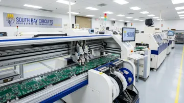
South Bay Circuits, for example, assembles down to 0.4mm-pitch BGA components on its SMT lines, a level of precision that's become standard for high-density digital and RF designs.
SMD vs. Through-Hole Assembly: Key Differences
The two technologies aren't really competitors anymore. They're tools for different jobs.
| Factor | SMD Assembly | Through-Hole Assembly |
|---|---|---|
| Component size | Sub-millimeter to a few mm | Larger, leaded packages |
| Assembly speed | High-speed automated placement | Slower, often manual insertion |
| Mechanical strength | Lower; relies on solder joint | Higher; leads pass through the board |
| Cost at scale | Lower per unit at volume | Higher labor cost per unit |
| Signal performance | Shorter leads, less parasitic loss | More lead length, more inductance |
Through-hole hasn't disappeared. Connectors, power components, and parts exposed to heavy vibration still often need the mechanical grip that plated through-holes provide. That's why hybrid assembly, combining SMD and through-hole on one board, remains standard practice rather than the exception.
Why the Industry Is Shifting Toward SMD
The numbers back up what's happening on the factory floor. The global SMT market was valued at $5.8 billion in 2023 and is projected to reach $8.4 billion by 2028, a 7.8% compound annual growth rate, according to MarketsandMarkets' 2023 industry analysis. That growth spans placement equipment, inspection systems, and assembly services alike.
Higher density and lower manufacturing cost at scale are the two forces driving that curve. Through-hole simply can't compete on either front once volumes climb.
The SMD PCB Assembly Process: From Design to Delivery
SMD assembly is a precision sequence, and each stage either sets up success or introduces risk for the next. Skip a step, or rush one, and defects tend to surface later, when they're far more expensive to fix.
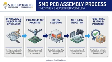
Step 1: DFM Review and Solder Paste Application
A Design for Manufacturability (DFM) review happens first, catching issues like insufficient pad clearance, silkscreen conflicts, or panelization problems before they become scrapped boards on the production line. Only then does solder paste get printed onto pads through a laser-cut stencil aligned to the PCB's footprint.
Step 2: High-Speed Pick-and-Place Mounting
Automated pick-and-place machines lift components from reels or trays and set them onto the pasted pads. Yamaha's YRM20 mounter, for instance, is rated for 115,000 components per hour with placement accuracy of ±25 micrometers, according to the manufacturer's 2020 launch specifications. That kind of throughput is what makes high-volume SMD production economically viable.
Step 3: Reflow Soldering
Populated boards travel through a multi-zone reflow oven, where separately controlled heating zones create a precise time-temperature profile. This profile has to match the solder alloy: leaded (SnPb) processes typically peak in the 220-235°C range, while lead-free profiles run hotter, generally 245-260°C, depending on package thickness and thermal mass.
Get the profile wrong and you risk cold joints on one end, scorched components on the other.
Step 4: Automated Optical and X-Ray Inspection
Once boards cool, AOI (Automated Optical Inspection) scans every joint for visible defects, tombstoning, where a chip component stands upright instead of sitting flat, solder bridges, misaligned parts, and missing components. But some defects hide beneath the package. X-ray inspection reveals what optical systems can't, checking BGA solder joints for voids, shorts, and poor wetting underneath the ball array.
Step 5: Functional Testing, Cleaning, and Final Packaging
The final stage confirms the board actually works. Flying probe or functional testing verifies electrical performance against design specs. Technicians then clean boards of flux residue, perform one final inspection, and package them for shipment or integration into a larger box build.
Key Benefits of Professional SMD PCB Assembly
The advantages of SMD go beyond just "smaller." Three factors matter most for engineering teams:
- Higher density. Package sizes as small as 0.6 x 0.3mm let designers fit far more circuitry into the same board footprint, critical for wearables, medical implants, and compact industrial controllers.
- Faster, cheaper production at scale. Automated placement lines process thousands of components per hour, which drives per-unit cost down as volume climbs, something manual through-hole assembly simply can't match.
- Better high-frequency performance. Shorter leads cut parasitic inductance, and Vishay's 2009 frequency response study found 0201 packages deliver the best impedance performance across 0.1–40 GHz.
That last point matters more than it might seem: for RF, high-speed digital, or signal-sensitive designs, component footprint directly affects electrical performance, not just available board space.
Common Challenges in SMD Assembly (and How Experts Solve Them)
SMD assembly isn't without its headaches. Here's what typically goes wrong, and how established manufacturers prevent it.
Component fragility. Parts as small as 0201 are easy to damage or misplace by hand. Automation prevents this kind of damage. Pick-and-place systems and trained technicians working under magnification keep handling errors out of the process.
High equipment costs. A single pick-and-place line, reflow oven, and stencil set can run into hundreds of thousands of dollars. Most OEMs don't need to own that equipment. Partnering with a contract manufacturer that already runs Fuji SMT lines in-house sidesteps the capital investment entirely.
Process drift. Solder voids, misalignment, and paste inconsistency creep in without tight controls. Statistical Process Control (SPC), paired with AOI and X-ray inspection at every stage, keeps defect rates low and catches drift before it becomes a shipped problem.
How to Choose the Right SMD PCB Assembly Partner
Not every contract manufacturer is built for the same workload. Here's what actually separates a reliable partner from a risky one.
Verify certifications that match your industry:
- ISO 9001:2015 - baseline quality management, applicable everywhere
- AS9100 - aerospace and defense programs
- ISO 13485 - medical device manufacturing
- IATF 16949 - automotive production
- ITAR registration - required for defense articles and services
South Bay Circuits holds ISO 9001:2015, ISO 13485, IATF 16949, and AS9100 certifications. Adding ITAR registration and CMMC Level 1 compliance covers the regulatory bases most OEM and defense programs need.
Single-source, in-house capabilities reduce risk. When design, fabrication, and assembly all happen under one roof, you eliminate the queue times, shipping delays, and finger-pointing that come with juggling multiple vendors. SBC runs design, fab, and assembly out of a single 60,000-square-foot Chandler, Arizona facility, which removes the handoff gaps that slow down multi-vendor builds.
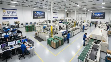
Turnaround capability matters too. Fast doesn't have to mean risky if the process controls are solid. SBC, for instance, offers PCB fabrication in as little as 24 hours and same-day assembly for urgent NPI and production runs.
Quality control stack should be complete, not optional. Look for:
- AOI (automated optical inspection) to catch assembly errors before boards leave the line
- X-ray inspection to verify BGA and fine-pitch solder joints hidden from view
- Functional testing to confirm boards perform as designed
A track record of industry quality awards is a useful signal too.
Experience and longevity count. SBC has operated continuously since 1981, over four decades of design-to-production work across aerospace, medical, automotive, and industrial programs. That kind of history tends to show up in fewer surprises during production ramp-up.
Industries and Applications Benefiting from SMD Assembly
High-reliability sectors depend on SMD assembly precision where failure isn't an option:
- Aerospace and defense - flight electronics, avionics, and defense systems requiring AS 9100 and ITAR compliance
- Medical devices - diagnostic equipment and implantables under ISO 13485
- Automotive - sensor modules and control units meeting IATF 16949 requirements (the successor to ISO/TS 16949)
- Industrial instrumentation - process controls and monitoring equipment
Compliance-driven industries need assembly partners whose certifications match the program, not just general quality claims. Consumer electronics and IoT devices lean on SMD assembly too, though for a different reason: compact, high-volume production runs where automation drives cost down fast.
Frequently Asked Questions
What is the difference between SMD and SMT?
SMT (Surface Mount Technology) is the overall manufacturing method used to assemble boards. SMD (Surface Mount Device) refers specifically to the components mounted using that method.
How long does SMD PCB assembly typically take?
Turnaround depends on complexity and volume. Quick-turn providers like South Bay Circuits can deliver prototypes in as little as same-day to 3 days, while standard production runs typically take one to two weeks.
Can SMD and through-hole components be combined on the same board?
Yes. Mixed assembly is standard practice for boards needing both compact SMDs and rugged through-hole connectors, using methods like selective soldering or pin-in-paste reflow.
What certifications should I look for in an SMD assembly provider?
Look for ISO 9001 as a baseline, plus AS9100 for aerospace, ISO 13485 for medical devices, IATF 16949 for automotive, and ITAR registration for defense work. South Bay Circuits holds all of these certifications.
Is SMD assembly more cost-effective than through-hole assembly?
Yes, especially at scale. Automation drives per-unit costs down significantly on higher-volume runs, though very low-volume jobs may see less of a cost advantage due to setup costs.
What quality checks are performed after SMD assembly?
Standard post-assembly checks include Automated Optical Inspection (AOI), X-ray inspection for hidden joints like BGAs, and functional or flying probe testing to confirm electrical performance.