
Introduction
A PCB's assembly-readiness gets decided long before it reaches the production floor. It gets locked in at layout: when you pick a footprint, set a clearance, or skip a stackup conversation with the fabricator.
Many designers still sign off a layout without DFA or DFM review. That gap shows up later as respins, missed ship dates, and a contract manufacturer left guessing at design intent.
This guide breaks down what actually makes a board assembly-ready. You'll get the core layout rules (including the often-misunderstood 3W rule), component placement best practices, the documentation your assembly partner needs, and how to pick a manufacturing partner that won't slow you down.
Key Takeaways
- Applying DFA principles during layout — not after — cuts rework, scrap, and time-to-market
- Clearance rules, the 3W rule, and minimum feature sizes decide whether a board is manufacturable or scrap
- Component placement, accurate footprints, and thermal design directly determine solderability and reliability
- Standardized BOM, Gerbers, and assembly notes prevent the back-and-forth that stalls NPI
- A certified, single-source partner shortens the path from finished design to loaded assembly
Understanding PCB Assembly Design (DFA) and Why It Matters
Before a single trace gets routed, designers should be asking one question: what makes this board assembly-ready, and what does getting it wrong actually cost?
What Is Design for Assembly (DFA) and How Does It Differ from DFM?
Design for Assembly (DFA) is the practice of laying out a board so components can be mounted and soldered efficiently and reliably. It covers pin-to-pad distance against reflow rules, component-to-component spacing for rework access, and related placement constraints.
Design for Manufacturing (DFM) is broader. It governs whether the bare board itself can even be fabricated : trace widths, drill sizes, layer registration, and similar constraints.
The two overlap constantly. A clearance violation, for instance, can break fabrication rules and assembly rules at the same time. That's why both checks need to happen together, before a design ever gets released to production , not sequentially and not as an afterthought.
How IPC Classes Shape Assembly Design Requirements
IPC-A-610 splits electronic assemblies into three classes based on how critical continued performance is, not simply on which industry you're in:
- Class 1 – General Electronic Products: Function matters; cosmetic imperfections don't
- Class 2 – Dedicated Service Electronic Products: Extended life and uninterrupted service expected, but not mission-critical
- Class 3 – High Reliability: Downtime isn't tolerable (flight-control or life-support systems)

Medical, automotive, and aerospace/defense programs frequently land in Class 3, but not automatically. Classification follows service criticality, not the industry label alone.
If your program needs that rigor, work with a manufacturer that holds the matching certifications. South Bay Circuits, for example, maintains ISO 13485 for medical, AS9100 for aerospace, and ISO/TS 16949 for automotive, plus IPC-A-610 Class 2 and Class 3 assembly capability.
Why Assembly-Friendly Design Impacts Cost, Quality, and Time-to-Market
The cost of catching a DFA issue gets steeper the later you catch it. An IPC-hosted paper citing Aberdeen Research found that designers using advanced DFM practices averaged 57% fewer revision spins — 1.2 per design versus 2.8 for everyone else — and saved roughly $20,800 in materials per design.
Those figures separate a single respin from three, and a hit launch window from a missed one. Catching DFA problems during layout, rather than after boards hit the line, compresses your NPI cycle and avoids the re-spin loop entirely.
PCB Layout and Routing Guidelines for Assembly-Ready Boards
Layout and routing choices decide whether a board assembles cleanly or fights every process step from fab through solder. The guidelines below keep geometry, spacing, and documentation inside real production limits.
Layer Stackup and Material Planning
Request your fabricator's stackup and material options before you place a single component. Designing around a stackup your fabricator can't build with the intended electrical performance means starting over.
Copper weight has to match current-carrying requirements, especially on power planes. IPC-2152 governs conductor sizing for current capacity, but copper weight alone doesn't tell the whole story. Current, permitted temperature rise, and trace width are linked variables you size together, not a single lookup number.
Copper-to-Copper Clearances and Drill Hit Spacing
Four clearance checks matter, and default ECAD software values are frequently too aggressive for real production:
- Trace-to-trace: Stay at or above fabricator minimums; prefer wider spacing when density allows
- Trace/pad-to-polygon: Set pour clearances so copper floods don't violate spacing
- Trace-to-pad: Leave enough gap for mask and clean solder joints
- Pad-to-pad: Check copper spacing and drill-hit separation as separate rules
South Bay Circuits, for reference, documents standard external trace/space of 0.004"/0.004" with ½-ounce copper, tightening to 0.003"/0.003" for advanced designs, but recommends 0.005" or greater whenever the design allows it. Tighter geometry adds cost without adding value on most boards.
Drill hits are a separate trap. Pad-to-pad spacing can look fine on screen while the actual drill hits still overlap, because pad size doesn't automatically scale with hole diameter. The fix: pad diameter should equal drill diameter plus roughly 8 mils. Skip that math and you'll find out about it after the board's already drilled.
Understanding the 3W Rule in PCB Routing
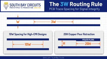
The 3W rule is a simple ratio: spacing between the centerlines of adjacent traces should be at least three times the trace width. That spacing helps contain each trace's electromagnetic field and cut crosstalk, especially on traditional stackups with thicker dielectric.
Crosstalk itself is driven by mutual capacitance and inductance between parallel traces. The closer traces run, and the longer they stay parallel, the worse it gets.
Where does it matter most?
- High-speed digital bus: 3W spacing is close to mandatory; tighter spacing invites signal integrity headaches that are painful to debug after fab
- Low-speed analog trace: 3W is still good practice, but the consequences of ignoring it are far less severe
For designs with stricter EMI requirements, some engineers extend spacing to 10W. For plane edges, the related 20H rule pulls the power-plane edge inward from the ground-plane edge by 20 times the plane-to-plane distance to reduce edge radiation.
Minimum Feature Sizes, Solder Mask, and Silkscreen Rules
Just because a fabricator can hit 3-mil trace/space doesn't mean your board should. Simpler designs should default to more conservative values, generally in the 8-10 mil range. Tighter geometry adds cost and yield risk without a functional payoff on boards that don't need it.
Solder mask and silkscreen rules matter just as much:
- Solder mask slivers need a minimum web width to avoid bridging risk between adjacent pads
- Silkscreen-to-pad clearance must keep ink off solderable copper; violations often show up as rejected boards at inspection, not in design review
Component Placement, Footprint, and Thermal Design Best Practices
A layout that passes every clearance check can still fail on the line if component placement wasn't designed for how the board actually gets built. This section translates a compliant layout into one that assembles cleanly.
Selecting the Right Mounting Technology (SMT, THT, or Mixed)
- SMT suits high-density, fine-pitch designs and dominates modern boards. SBC's automated lines handle SMD packages down to 0201 as standard, with fine-pitch placement to 0.4mm under engineering review
- Through-hole still makes sense for parts needing mechanical strength or high current, such as connectors and power components, and supports both wave and hand soldering
- Mixed technology combines both on one board, which is common when connectors sit alongside dense SMT fields
Component Placement, Orientation, and Spacing Rules
Polarity and orientation markings need to be visible and unambiguous, not just present. Keep-out zones around connectors matter too, since pick-and-place equipment and inspection tools (AOI, X-ray) need physical access to every joint.
For dense BGA fields, that access requirement isn't cosmetic. If AOI or X-ray equipment can't get a clean view or angle, you lose your ability to verify hidden solder joints, which is exactly where BGA failures hide.
Footprint and Land Pattern Accuracy
Incorrect footprints, meaning ones that don't follow IPC-7351 land pattern standards, are a direct path to tombstoning, solder bridging, or component misalignment during reflow. This is especially common on small passives like 01005 packages, where even minor pad asymmetry causes one end of the component to lift during reflow.
Verify the exact package drawing and pin-to-pad relationship against your assembler's reflow rules, not just the datasheet's suggested footprint.
Thermal Vias and Heat-Sensitive Component Placement
Power components need a path to move heat out of the board. According to TI's thermal design guidance, thermal vias inside the exposed pad (about 0.3 mm or smaller on roughly 1 mm spacing) with full-circumference plane connections move heat from top copper to inner and bottom layers more effectively than thermal-relief spokes.
One caution: too much solder flowing through internal vias during reflow can cause voiding. Plugging prevents it but adds cost. Discuss that tradeoff with your fabricator before it becomes a surprise.
Heat-sensitive components (anything with tight thermal tolerances) should sit away from these hot zones entirely. Uninterrupted copper area for heat spreading matters more than copper thickness alone.
Reference Designators and Pin 1 Marking
Legible reference designators and clear Pin 1 markings matter for manual assembly, rework, and inspection traceability. A silkscreen label that's too small to read under a microscope defeats its own purpose.
Documentation and Files Your PCB Assembly Partner Needs
Every assembly house needs a complete, unambiguous package. Missing or conflicting data is one of the most common reasons a design stalls before it ever reaches the line.
Core file package:
- Gerber or ODB++ files — complete layer set, typically 274X/RS274X format
- Bill of Materials (BOM) — full part numbers, revisions, and package details, usually delivered in Excel
- Assembly drawing — component orientation, height limits, and board-side identification
- Pick-and-place (centroid) data — X-Y coordinates, rotation, and board side for every component
- Excellon drill data — for hole locations and sizes
Assembly notes cover what drawings can't fully capture:
- Mounting method per IPC-CM-770 and soldering requirements per J-STD-001
- Special installation steps, ESD handling, and conformal coating callouts
- Final test acceptance criteria
Before committing to production, request a DFM/DFA check from your manufacturer. It's the cheapest insurance available against missing netlists, conflicting tolerances, or a footprint nobody caught until the line stopped.
Choosing the Right PCB Assembly Manufacturing Partner
A single-source provider (one that handles design support, fabrication, and assembly under one roof) eliminates the queue and ship time that stacks up between separate vendors. That transfer time between suppliers can end up longer than the actual processing time for any individual step.
South Bay Circuits has run this model since 1981 from a 60,000+ square-foot Chandler, Arizona facility, moving from finished design and layout to fabrication and assembly in as little as 48 hours when a project is ready.

When evaluating a partner, match their certifications to your industry before you sign anything:
| Industry | Certification to Confirm |
|---|---|
| Aerospace & defense | AS9100, ITAR registration |
| Medical | ISO 13485 |
| Automotive | ISO/TS 16949, PPAP capability |
| General/baseline | ISO 9001:2015 |
Turnaround is a competitive factor for NPI programs. A partner offering 24-hour fabrication and same-day assembly (SBC's published quick-turn benchmark) can compress a schedule that would otherwise take weeks with a multi-vendor setup.
That speed only pays off if your documentation package is complete going in. Skipping the DFM/DFA check to save a day upfront tends to cost several days later.
Frequently Asked Questions
What is the 3W rule in PCB routing?
The 3W rule requires spacing between adjacent trace centerlines to be at least three times the trace width. This helps contain each trace's electromagnetic field and reduces crosstalk between neighboring signals.
What are the guidelines for PCB layout?
Layout guidelines cover layer stackup planning, copper clearances, minimum feature sizes, component placement and orientation, and solder mask/silkscreen rules. Together, these ensure the board can be fabricated and assembled reliably.
What is the difference between DFM and DFA in PCB design?
DFM verifies that the bare board can actually be fabricated: trace widths, drill sizes, layer registration. DFA verifies that components can be mounted and soldered onto that board efficiently and reliably. Check both before you release the design.
What documents are required for PCB assembly?
Standard packages include Gerber or ODB++ files, a bill of materials, an assembly drawing, pick-and-place (centroid) data, and assembly notes covering mounting method and soldering requirements.
What is the minimum trace width and spacing for PCB assembly?
Advanced processes can reach 3-4 mil trace/space, while simpler, cost-sensitive designs typically use 8-10 mil for better yield and lower cost. Always confirm exact limits with your chosen manufacturer before finalizing layout.
How early should I involve my PCB assembly manufacturer in the design process?
Bring your manufacturer in during stackup planning and before finalizing layout, so DFM/DFA review happens while changes are still cheap. Waiting until after layout is locked in drives costly redesigns.