Key Takeaways
- PCB assembly transforms a bare fabricated board into a working electronic device by soldering components using SMT, through-hole, or hybrid techniques
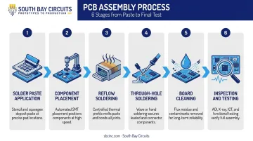
- The process follows a defined sequence: solder paste application → component placement → reflow soldering → through-hole soldering → cleaning → inspection → testing
- Quality control happens at multiple stages — AOI, X-ray, and functional testing catch defects early and protect first-pass yield
- Complete documentation (BOM, Gerber files, pick-and-place data) reduces errors and speeds turnaround
- A single-source partner handling fabrication and assembly eliminates coordination overhead and cuts time to market
What Is Electronic PCB Assembly?
PCB assembly is the process of mounting and soldering electronic components — resistors, capacitors, ICs, connectors, and more — onto a fabricated printed circuit board to create a complete, functional electronic circuit.
Two terms are easy to confuse here:
- PCB fabrication — manufacturing the physical board itself (drilling, plating, etching, lamination)
- PCB assembly (PCBA) — populating that bare board with components and soldering them in place
The finished result is called a PCBA (Printed Circuit Board Assembly). Once assembled, the conductive traces and pads on the board carry electrical signals between all mounted components, making the board a functional part of a larger electronic system.
In the broader electronics manufacturing lifecycle, assembly sits between fabrication and final product integration. It comes after the schematic is designed and the bare board is built, but before the PCBA is installed into its enclosure or system.
The Electronic PCB Assembly Process, Step by Step
Modern assembly follows a sequential, structured workflow across six core stages. Each step builds on the previous one, and automated equipment paired with skilled technician oversight drives the high-accuracy, high-volume output that today's OEM programs demand.
Solder Paste Application
A metal stencil is aligned over the bare PCB. Solder paste — a mixture of powdered solder alloy and flux — is spread across it using a squeegee, depositing paste precisely onto each component pad.
Stencil alignment accuracy is critical. Even slight misalignment causes solder bridges or weak joints downstream. Modern stencil printers achieve tight tolerances: ASMPT's DEK TQ, for example, specifies ±17.0 µm at 2 Cpk wet-print accuracy — though these are machine-specific figures, not universal industry tolerances.
Component Placement
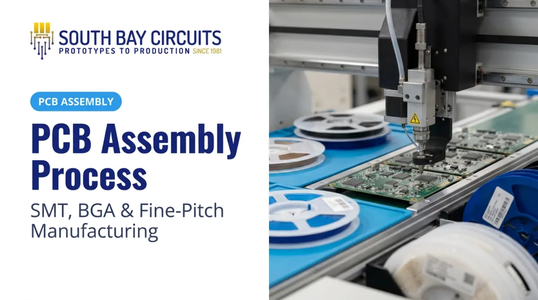
Pick-and-place machines automatically remove components from reels or trays and position them onto the solder-pasted pads using pre-programmed X-Y coordinates and vision alignment systems. High-end placement platforms such as the Yamaha YRM20DL achieve up to 120,000 components per hour at ±0.015 mm accuracy (3 sigma) — performance figures that vary by platform and process configuration.
For small-volume or complex prototype runs, manual placement under magnification can supplement automated placement where needed.
Reflow Soldering
Boards travel through a multi-zone reflow oven following a controlled temperature profile — preheat, soak, reflow peak, and cooling — that melts the solder paste and forms permanent electrical and mechanical joints.
Profile parameters vary by solder chemistry. Lead-free SAC305 paste typically requires a 230–260°C peak temperature, while leaded Sn63Pb37 processes generally peak at 210–230°C. Profile optimization matters — excessive ramp rates can cause solder balls or bridging, while insufficient heat produces cold joints.
Through-Hole Component Soldering
After SMT reflow, any through-hole (PTH) components — large connectors, transformers, power components — are inserted into drilled holes and soldered. The method depends on complexity and thermal sensitivity:
- Wave soldering — efficient for high-volume runs; the board passes over a molten solder wave that simultaneously solders all through-hole joints
- Selective soldering — targets specific joints, uses less material than wave, and is faster than hand soldering
- Hand soldering — appropriate for localized attachment, rework, or low-volume builds
Board Cleaning
Post-solder cleaning removes flux residues and contaminants using deionized water, solvent-based solutions, or aqueous chemistry. The right cleaning method depends on the flux type and component compatibility — as outlined in IPC-CH-65B, the industry guideline for post-solder cleaning.
No-clean flux options exist for non-washable components, skipping the cleaning step to protect sensitive parts. However, no-clean residues may still require removal when reliability requirements, conformal coating adhesion, or test probing demands a clean surface.
Inspection, Testing, and Final Quality Verification
After assembly, boards go through multi-stage quality checks — covered in detail in the Quality Control section below.
Types of Electronic PCB Assembly
The assembly method chosen depends on component types, board complexity, production volume, and end-use environment. Three main approaches cover most designs.
Surface Mount Technology (SMT) Assembly
SMT is the dominant modern assembly method. Components (SMDs) mount directly onto the board surface rather than inserting through holes. Key advantages:
- Supports smaller, lighter, higher-density board designs
- Compatible with high-speed automated placement and reflow
- Well-suited for mass production and consistent repeatability
- Standard in consumer electronics, medical devices, and telecommunications equipment
Per an IPC-hosted Indium Corporation paper, SMT has dominated through-hole technology since the early 1990s because of higher component density and lower ultimate cost.
Through-Hole Technology (THT) Assembly
THT inserts component leads through drilled holes in the PCB and solders them to pads on the opposite side. This creates stronger mechanical bonds than surface mounting. That mechanical advantage is why THT remains preferred for:
- High-vibration environments (aerospace, military)
- High-power applications (power electronics, industrial controls)
- Situations where component retention under physical stress is critical
That same Indium paper notes that through-hole solder joints improve strength and reliability in server, telecom, and automotive applications.
Hybrid (Mixed-Technology) Assembly
Hybrid assembly combines SMT and THT on a single board. It's the right approach when a design needs SMT density for smaller components alongside THT durability for large or high-power parts.
Typical sequence:
- SMT components are placed and reflow-soldered first
- Through-hole components are inserted and soldered using wave or selective methods
- Completed assemblies undergo inspection to verify solder joint integrity across both technologies
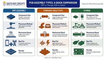
Hybrid boards appear frequently in power supplies, automotive electronics, and industrial control systems where both density and mechanical robustness matter.
Quality Control and Inspection in PCB Assembly
Quality assurance runs through every stage of PCB assembly, not just a final pass at the end of the line. IPC-A-610J (released in 2024) defines post-assembly acceptance criteria, while J-STD-001J governs soldering processes and materials. Together, these standards define what "acceptable" looks like at every stage.
Automated Optical Inspection (AOI)
AOI systems use high-resolution cameras and image-recognition software to compare each assembled board against a reference, automatically flagging:
- Missing or misoriented components
- Solder bridges and insufficient solder
- Wrong component values or polarity
AOI is deployed after both SMT reflow and final assembly to catch visible defects early. Modern systems offer optical resolution in the 8–15 µm range, enabling detection of fine surface-level defects.
X-Ray Inspection
AOI can't see underneath components. X-ray inspection is used for hidden solder joints — BGAs, QFNs, flip-chips — where optical access is impossible. X-ray reveals:
- Internal voids in solder joints
- Incomplete or cold joints
- Shorts that wouldn't surface until electrical failure
This is a non-destructive inspection method, making it practical for 100% inspection of high-reliability boards with dense or complex packages.
Functional and In-Circuit Testing
Two electrical verification methods confirm a board performs as designed:
- ICT (In-Circuit Testing) — uses test probes to check individual components and connections for shorts, opens, and component value accuracy. Bed-of-nails fixtures cover high-volume programs; flying-probe systems avoid the need for a dedicated fixture.
- FCT (Functional Circuit Testing) — simulates real operating conditions to verify system-level behavior under powered conditions.
Testing methodology must match the board's complexity and the reliability requirements of its end application.
Certifications That Signal Quality Standards
Certifications indicate that a supplier operates under documented, audited quality management processes — not just informal practices. Relevant standards for PCB assembly:
| Certification | Scope |
|---|---|
| ISO 9001:2015 | Organization-wide quality management; applicable to any sector |
| ISO 13485 | Medical device production; emphasizes traceability and process validation |
| AS9100 | Aviation, space, and defense QMS requirements |
| ISO TS 16949 | Automotive quality management and production part approval |
| ITAR Registration | Required for defense and controlled-technology programs |
| CMMC Level 1 | Cybersecurity Maturity Model Certification for defense supply chain |
South Bay Circuits holds ISO 9001:2015, ISO 13485, AS9100, and ISO TS 16949 certifications, with ITAR registration and CMMC Level 1 compliance. For aerospace, defense, medical, and automotive programs, these credentials confirm that quality traceability is built into every documented process — not assumed.
What Files and Information Do You Need to Start PCB Assembly?
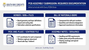
Incomplete documentation is one of the most common causes of assembly delays. Before kicking off any job, an assembler needs four core data sets:
| Document | Contents |
|---|---|
| Gerber / ODB++ files | Board geometry and layout data establishing the physical assembly substrate |
| Bill of Materials (BOM) | Component list with reference designators, part numbers, and quantities |
| Pick-and-place / centroid file | X, Y coordinates, rotation angle, and board side for each placed component |
| Assembly notes / drawings | Special handling requirements, solder type preferences, non-washable component callouts, polarity markings |
A clean BOM with verified part numbers, correct quantities, and unambiguous alternates reduces the risk of wrong components being sourced or placed. It also enables a DFA (Design for Assembly) review before production starts, catching potential manufacturing issues at the design stage rather than mid-run.
That same data integrity logic extends to your file format choice. As Siemens describes it, ODB++ is a single structured data set spanning fabrication, assembly, and test — capturing board geometry, component placement, and test data in one format, which reduces the risk of data mismatches between tools.
Choosing the Right Electronic PCB Assembly Partner
Not all assembly partners offer the same capabilities, and the right choice depends on what your project actually requires. Key factors to evaluate:
- Assembly capabilities — SMT, THT, hybrid, BGA fine-pitch support
- Certifications — ISO 9001:2015 minimum; ISO 13485 or AS9100 for regulated industries
- Component sourcing model — turnkey (assembler sources components) vs. consigned (customer supplies parts)
- Inspection capabilities — AOI, X-ray, ICT, FCT in-house vs. outsourced
- Turnaround time — especially for prototype and NPI cycles
Single-Source vs. Split-Vendor
Working with a partner that handles both PCB fabrication and assembly under one roof eliminates the coordination overhead that arises when fab and assembly are split across vendors. When one vendor builds the board and another assembles it, delays at the handoff — and finger-pointing when defects occur — become predictable problems.
Domestic Assembly for Controlled Programs
US-based assembly matters for programs involving ITAR-controlled technologies, where foreign-person access to technical data must be managed. Under 22 CFR 122.1, manufacturers of defense articles must register with DDTC — and working with a registered domestic assembler simplifies compliance.
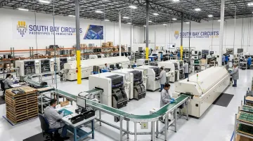
South Bay Circuits operates from a 60,000+ sq. ft. facility in Chandler, Arizona, with ISO 9001:2015, ISO 13485, AS9100, and ITAR registration. SBC offers 3-Day Turn or Less assembly and 24-hour bare board fabrication, providing a verified single-source path from design files through loaded assembly. That combination is especially relevant for teams managing tight NPI timelines or defense-related programs.
Turnaround as a Competitive Factor
In product development, the cycle from design files to assembled boards directly affects how fast a team can iterate. A partner that compresses prototype turnaround from weeks to days doesn't just save time. Faster boards mean faster design validation — and a shorter path to production.
Frequently Asked Questions
What is electronic board assembly?
Electronic board assembly (also called PCB assembly or PCBA) is the process of mounting and soldering electronic components onto a printed circuit board to create a functional device. Unlike PCB fabrication — which produces the bare board — assembly begins once that board is ready to be populated with components.
How are electronic boards assembled?
Solder paste is applied to the board via a metal stencil, components are placed by pick-and-place machines, and the board passes through a reflow oven to solder SMT components. Through-hole parts are soldered separately using wave, selective, or hand methods. The board is then cleaned, inspected with AOI and X-ray, and tested before shipment.
How much does electronic board assembly cost?
PCB assembly cost varies based on several factors:
- Board complexity and layer count
- Component count and assembly type (SMT, THT, or hybrid)
- Production volume and turnaround requirements
No standard price applies across all builds. Request a quote with your design files and BOM for accurate pricing.
What is the difference between SMT and through-hole PCB assembly?
SMT mounts components directly on the board surface, enabling high-density automated assembly suited to most modern electronics. Through-hole technology inserts component leads through drilled holes for stronger mechanical bonds, preferred in high-stress or high-vibration applications. Many production boards use a hybrid of both.
What files are needed to submit for PCB assembly?
Four files are required for most assembly submissions:
- Gerber or ODB++ fabrication files
- Bill of Materials (BOM) with part numbers and reference designators
- Pick-and-place (centroid) file with component coordinates
- Assembly notes for special handling or process requirements
Complete documentation speeds up quoting and prevents delays at assembly start.