Standard PCB technology runs out of room fast. Once you're routing fine-pitch BGAs and dense mixed-signal circuits on a conventional board, through-hole vias and wide trace spacing start eating up real estate you don't have. That's the wall that pushes designers toward High-Density Interconnect, or HDI, construction.
This guide breaks down what HDI actually means, the design rules that govern it, and where it shows up in real products. Whether you're specifying your first HDI board or refining a stack-up for a fine-pitch design, you'll find the practical detail you need here.
Key Takeaways
- HDI boards achieve higher wiring density through microvias, finer traces, and sequential lamination, not just more layers
- Microvia aspect ratio should stay at or below 1:1 to avoid plating voids and long-term reliability failures
- Stack-up notation (0-N-0, 1-N-1, 2-N-2) directly drives both routing density and fabrication cost
- Material choice affects laser-drillability, signal loss, and thermal performance, especially for RF and high-speed designs
- Medical, aerospace, automotive, and industrial designs use HDI when space, weight, and reliability rule out conventional boards
What Is an HDI PCB?
An HDI PCB packs more wiring density into the same footprint than a conventional multilayer board. It does this through microvias, thinner traces and spacing, and additional layers built up in a smaller area.
The result is a board that performs the same electrical function as a standard multilayer design, often with fewer total layers, in a smaller and lighter package. That's the whole point of HDI: not just squeezing in more circuitry, but doing it more efficiently.
HDI vs. Standard PCB
The differences show up in a few key areas:
| Feature | Standard PCB | HDI PCB |
|---|---|---|
| Via type | Mechanically drilled through-hole vias | Laser-drilled microvias, plus blind/buried vias |
| Trace width/spacing | Typically 4-6 mil or wider | Often 3-4 mil, down to 2 mil on advanced builds |
| Via connections | Vias pass through the entire board | Microvias connect only selected adjacent layers |
| Layer efficiency | More layers needed for equivalent routing | Fewer layers can achieve the same routing density |
Smaller vias and pads free up copper real estate around each pad. That extra room is what lets you place fine-pitch BGAs and tightly spaced components that a standard board simply can't fit.
IPC Standards Governing HDI Design
A few IPC documents form the backbone of HDI design practice:
- IPC-2226 — Sectional design standard covering HDI board and microvia design rules, used alongside IPC-2221
- IPC/JPCA-2315 — A design guide covering HDI structure selection, materials, and microvia technologies
- IPC/JPCA-4104 — Material qualification requirements for conductive and dielectric materials used in HDI builds
- IPC-6016 — Originally the performance specification for HDI layers and boards, now folded into IPC-6012, IPC-6013, and IPC-6018 coverage
IPC's revision table currently lists 2226, 2315, and 4104 as "no longer maintained." Designers and fabricators still reference them heavily, but you should confirm current requirements with your fabricator rather than treating any single document as the final word.
Key HDI Specifications to Know
Based on IPC density criteria, manufacturers commonly use these thresholds to classify a board as HDI:
- Line/space: 100 microns (about 3.94 mil) or tighter
- Via diameter: under 150 microns (about 5.91 mil)
- Capture pad size: under 400 microns (about 15.75 mil)
These are useful benchmarks, but they vary by fabricator, so verify current capability numbers with your manufacturing partner rather than assuming a universal cutoff.
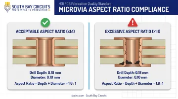
The microvia aspect ratio (drill depth divided by diameter) is equally critical. Industry guidance keeps this at or below 1:1, with many fabricators targeting closer to 0.8:1 for reliability margin.
Exceed that ratio and copper plating struggles to reach the bottom of the via evenly. The resulting voids concentrate stress during thermal cycling and eventually crack.
HDI PCB Design Guidelines
Getting HDI right comes down to four connected decisions: stack-up, vias, materials, and signal/power integrity. Get one wrong and it undermines the others.
Stack-Up Planning
HDI stack-ups use a shorthand notation that tells you how many sequential lamination cycles a board requires:
- 0-N-0 — A single lamination cycle with N core layers and no added buildup
- 1-N-1 — One sequential buildup layer added to each side of the core, adding two copper layers total
- 2-N-2 — Two sequential buildup laminations per side, adding four copper layers total
More buildup cycles mean more routing density, but they also mean more manufacturing steps, longer cycle times, and higher cost. Most designs land in the 2-to-3 lamination range as a practical balance.
Via Technologies and Aspect Ratio
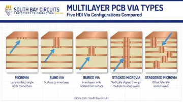
HDI boards typically combine several via types:
- Microvias — laser-drilled, connecting only adjacent layers, limited to roughly 1:1 aspect ratio
- Blind vias — connect an outer layer to inner layers without passing through the whole board
- Buried vias — connect inner layers only, invisible from either surface
- Stacked microvias — aligned vertically for dense fanout, but riskier past two levels
- Staggered microvias — offset laterally, generally more reliable for three-plus via layers
For fine-pitch BGA fanout, staggered microvias tend to work well at 0.5mm pitch, while stacked "inverted pyramid" routing handles 0.4mm and finer pitches.
SBC's manufacturing capabilities include general hole aspect ratios ranging from 10:1 for standard builds up to 16:1 for advanced builds, with microvia diameters as small as 0.004 inches. The 16:1 figure is an overall hole aspect ratio, not a universal microvia limit, so confirm what applies to your via structure during design review.
Material Selection for HDI
Dielectric choice affects three things: how well the laser drills through it, how much signal loss you get at your operating frequency, and how it holds up thermally over the product's life. Rough tiers look like this:
| Laminate Type | Best For | Key Trait |
|---|---|---|
| Standard/high-Tg FR4 | General-purpose, lower-speed digital | Cost-effective, widely available |
| Mid-loss laminates (such as Nelco N4000 series) | Moderate-speed digital, mixed signal | Better loss performance than FR4 |
| Low-loss RF/microwave laminates (such as Rogers, Isola Astra) | High-speed digital, RF/microwave | Low dielectric loss, tighter Dk control |
Check dielectric constant (Dk) and glass transition temperature (Tg) against your frequency and thermal targets before locking the stack-up. A material that drills beautifully but can't handle your thermal cycling profile will cost you more in field failures than it saved in fabrication.
Signal and Power Integrity Best Practices
Dense layouts amplify signal integrity problems if you're not deliberate about a few fundamentals:
- Controlled impedance: Finalize layer order, dielectric thickness, and copper geometry together — they all affect impedance simultaneously
- Differential pair matching: Route pairs on the same layer where possible and match length within your interface's tolerance
- Reference planes: Keep solid, continuous ground/power planes adjacent to high-speed layers
- Decoupling placement: Position capacitors close to ICs and minimize the loop formed by capacitor, vias, and planes
Via-to-via separation often matters more for decoupling performance than the trace length between capacitor and via, an easy detail to overlook when board space is tight.
Design for Manufacturability (DFM) Considerations
HDI's tight tolerances leave almost no room for guesswork. Bringing your fabricator into the conversation early, before the layout is locked, is the single best way to avoid a costly respin.
Common DFM issues that trip up HDI designs:
- Aspect ratio violations: specifying via depths that exceed what the fabricator can reliably plate
- Unsupported via-in-pad fill: designing for filled and capped microvias without confirming the fabricator's fill and planarization process
- Insufficient annular ring: leaving too little copper around a via after drilling tolerance and registration shift
At SBC, design, fabrication, and assembly happen under one roof at the Chandler, Arizona facility. That single-source setup matters for HDI work specifically because these boards involve dense layouts, controlled impedance, fine-pitch BGAs, and sequential lamination.
A mismatched handoff between separate design and fabrication vendors can introduce errors in any of those areas. Keeping the process integrated means DFM feedback comes from the same team that will actually build the board.
Applications of HDI PCBs Across Industries
HDI adoption tracks closely with industries that need both miniaturization and reliability. Industry-wide, HDI usage has grown substantially. IPC's 2023 PCB Technology Trends Report found that HDI fabrication rose from 37.5% to just over 49% of surveyed manufacturers' output over five years.
Industries that rely on HDI most include:
- Medical devices: wearables and implantables where board space is measured in millimeters
- Aerospace and defense: avionics and guidance systems that need density and long-term reliability
- Automotive: ADAS and infotainment modules packing sensor fusion and processing into tight housings
- Industrial and instrumentation: dense sensor and control functions in compact enclosures
Sourcing HDI boards for regulated markets means matching certifications to the application. SBC holds ISO 13485 compliance for medical device production, AS9100 for aerospace and defense, and ISO/TS 16949 for automotive. Those credentials matter when qualifying a fabrication partner for regulated HDI work.
Across these sectors, the driver is the same: more function in less space, without giving up reliability. Boards that once fit on standard multilayers increasingly need HDI just to stay inside the enclosure.
Benefits of HDI PCB Design
The case for HDI comes down to three measurable advantages.
Space and weight savings. Fewer layers doing the same routing job means a thinner, lighter board, which matters for wearables, implants, and airborne systems. IPC's advanced microvia design research documented a case where an 18-layer through-hole board became a 10-layer HDI design, cutting size and cost by nearly 40% while also improving signal integrity.
Signal integrity gains. Shorter trace lengths and reduced via stubs cut parasitic inductance. That same IPC research found a 2-mil-deep, 1-mil-diameter microvia carried less than 10 pH of self-inductance, versus nearly 200 pH for a comparable through via.
At high switching speeds, that gap is the difference between clean edges and a board that fails timing or EMI limits.
Higher component density. A 1089-pin, 1.0 mm-pitch BGA in the same study needed 20 through-hole layers versus 14 HDI layers for equivalent routing. That is six fewer layers and far more escape routing in the same footprint.
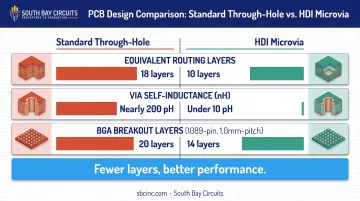
Fewer layers, tighter routing, and better electrical performance explain why HDI keeps showing up in new product categories each year.
Choosing the Right HDI PCB Manufacturing Partner
Design rules only get you halfway there. HDI's tight tolerances mean the fabricator's actual process capability matters just as much as what's on the layout file.
Look for a partner offering:
- Proven microvia and laser-drilling capability: demonstrated production experience at your target via diameter and aspect ratio, not just a spec sheet claim
- Quick-turn fabrication and assembly: HDI prototyping benefits from fast iteration when a design needs adjustment
- Quality certifications matched to your industry: medical, aerospace, automotive, and defense buyers all have distinct compliance requirements
South Bay Circuits has operated as a single-source PCB design, fabrication, and assembly partner since 1981 from a 60,000-square-foot facility in Chandler, Arizona. SBC's HDI-relevant capabilities include:
- Blind and buried vias, plus microvias down to 0.004 inches
- Sequential lamination, back-drilling, and conductive or non-conductive via fill for via-in-pad
- Boards from double-sided up to 22 layers, with trace/space as tight as 0.003"/0.003"
SBC holds ISO 9001:2015, ISO 13485, AS9100, and ISO/TS 16949 compliance, along with ITAR registration and CMMC Level 1 status. That coverage spans medical, aerospace/defense, and automotive sourcing requirements under one roof. Because design, fabrication, and assembly stay in the same facility, HDI projects move from layout review to loaded assembly without multi-vendor handoff delays.

If you're working through an HDI stack-up or need a DFM review before committing to fabrication, contact SBC to talk through your project.
Frequently Asked Questions
What is HDI in PCB design?
HDI, or High-Density Interconnect, is a PCB construction technique that achieves higher wiring density using microvias, finer traces and spacing, and additional buildup layers. It packs more circuitry into a smaller footprint than a conventional multilayer board.
What is the difference between HDI and a standard PCB?
Standard PCBs use mechanically drilled through-hole vias and wider trace spacing, typically requiring more layers for dense routing. HDI boards use laser-drilled microvias and tighter traces, often achieving the same electrical function with fewer layers.
What IPC standards apply to HDI PCB design?
The primary references are IPC-2226 for design rules, IPC/JPCA-2315 for HDI structures and microvia guidance, and IPC/JPCA-4104 for dielectric material qualification. Performance specifications fall under IPC-6012, 6013, and 6018.
What is aspect ratio in HDI via design, and why does it matter?
Aspect ratio is the microvia's drill depth divided by its diameter. Ratios above roughly 1:1 make it difficult for copper plating to reach the via bottom evenly, creating voids that cause reliability failures under thermal stress.
Which industries rely most on HDI PCBs?
Medical devices, aerospace and defense, automotive, and industrial/instrumentation equipment lead HDI adoption. Each combines a need for miniaturization with strict reliability requirements that HDI construction supports well.
Are HDI PCBs more expensive than standard PCBs?
Yes. Sequential lamination, laser drilling, and finer tolerances add cost versus standard boards. Space savings, weight reduction, and better signal performance usually offset that premium.