Introduction
A PCB assembly line is the coordinated sequence of automated and manual steps that turns a bare, fabricated circuit board into a fully populated, soldered, and tested electronic assembly. What looks straightforward on paper still depends on machine settings, inspection gates, and handoffs that decide whether boards pass or fail in the field.
This breakdown is written for engineers, procurement managers, and OEMs working in industrial, medical, aerospace/defense, automotive, and military electronics. If your boards must meet strict reliability and compliance standards, treating PCB assembly as a black box risks yield loss, delayed NPI, and compliance gaps that show up late in production.
Most people outside manufacturing use the term loosely without understanding what actually happens machine-by-machine. Below, we break down how the process works, what shapes output quality, where it fits into a production cycle, and when a full line isn't even the right call.
Key Takeaways
- PCB assembly turns a bare fabricated board into a functional assembly through paste, place, solder, and inspect steps
- Automated lines deliver consistency and repeatability that manual assembly cannot match at volume
- A full line runs five stages—prep, placement, soldering, inspection, and finishing—each gated before the next
- Component type, board complexity, and compliance requirements determine how a line is configured
- Prototypes and ultra-low-volume builds often need simplified or manual methods instead of a full line
What Is the PCB Assembly Line Process and Why It's Used
What Is the PCB Assembly Line Process?
PCB assembly is the manufacturing sequence that mounts, solders, and verifies electronic components on a bare printed circuit board so it functions as a working assembly. The outcome is straightforward: a board that reliably conducts signals and power exactly as designed, ready to drop into a finished device.
Assembly and fabrication get confused constantly, so the distinction matters:
- Fabrication builds the bare board: copper layers, drilling, lamination, etching
- Assembly places and solders components onto that already-finished board
One produces a blank canvas. The other makes it functional.
Why the Process Is Used in Electronics Manufacturing
Manual placement simply can't keep pace with modern component densities. Consider that Yamaha's YRM10 placement equipment, released in January 2024, is rated for up to 52,000 components per hour at ±35 micron accuracy under optimal conditions. No bench technician placing parts by hand approaches that throughput or repeatability on a fine-pitch board.
Regulated industries also demand things a manual process struggles to guarantee consistently:
- Medical devices require solder joint reliability aligned with ISO 13485
- Aerospace and defense need documented traceability and robustness under AS9100
- Automotive requires durability against vibration and thermal cycling per IATF/ISO TS 16949
South Bay Circuits, for example, holds ISO 9001:2015 certification through UL-DQS and maintains compliance with ISO 13485, AS9100, and IATF/ISO TS 16949 requirements. That lets medical, aerospace, and automotive customers stay with one vendor instead of routing each vertical elsewhere.
Without a controlled line, problems compound fast: misaligned components, solder bridges, batch-to-batch inconsistency, and field failures that cost far more to fix after shipment than on the line. Structured assembly is best practice across electronics manufacturing. In regulated sectors, it is also tied directly to IPC standards and quality systems like ISO 9001:2015.
How the PCB Assembly Line Process Works (Step-by-Step)
A bare board and a bill of materials (BOM) enter the line. The line places, solders, and verifies components. A functional assembly exits. Inputs include:
- A fabricated PCB
- Sourced components (in tape/reel, tray, or bulk packaging)
- Solder paste
- Assembly notes and BOM data
The core transformation happens through paste deposition, precision placement, and thermal bonding. Reflow temperature profiles, vision-guided placement accuracy, and inline inspection feedback loops control each stage. Here's how that plays out station by station.
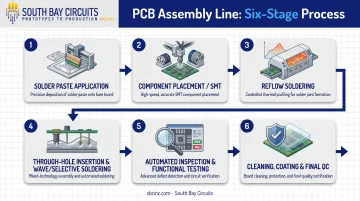
Step 1 — Solder Paste Application
A stencil printer applies solder paste onto the component pads, creating both a temporary adhesive and the future electrical connection. Solder paste inspection (SPI) then checks paste volume and alignment before placement, catching print defects before they become soldering defects downstream.
Step 2 — Component Placement (SMT)
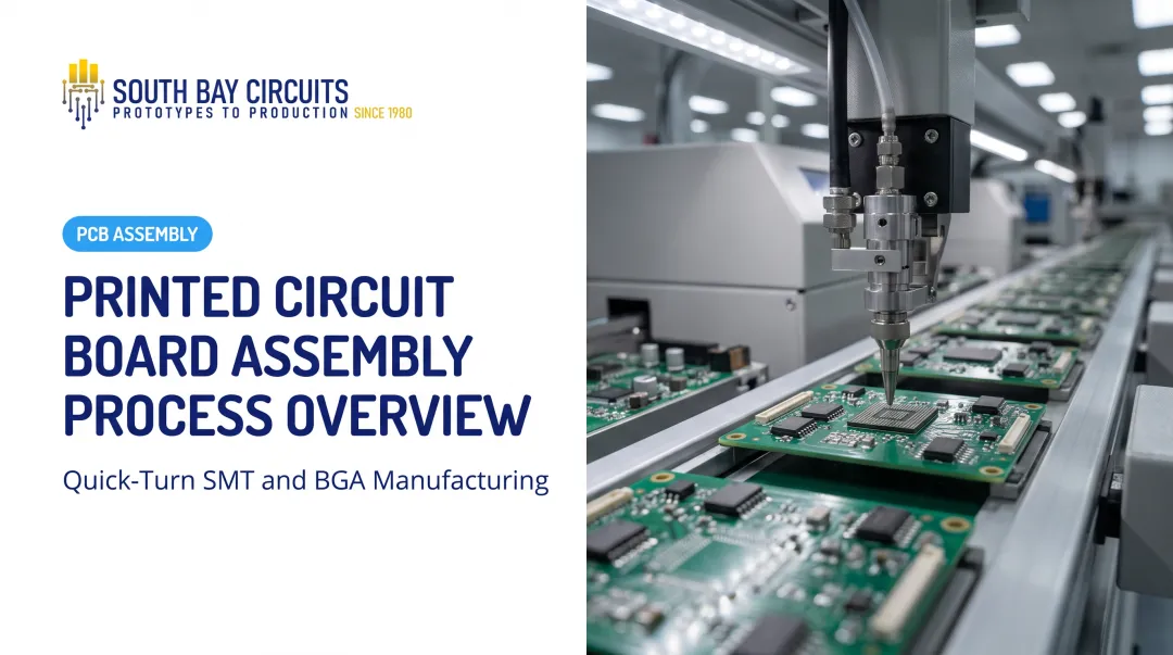
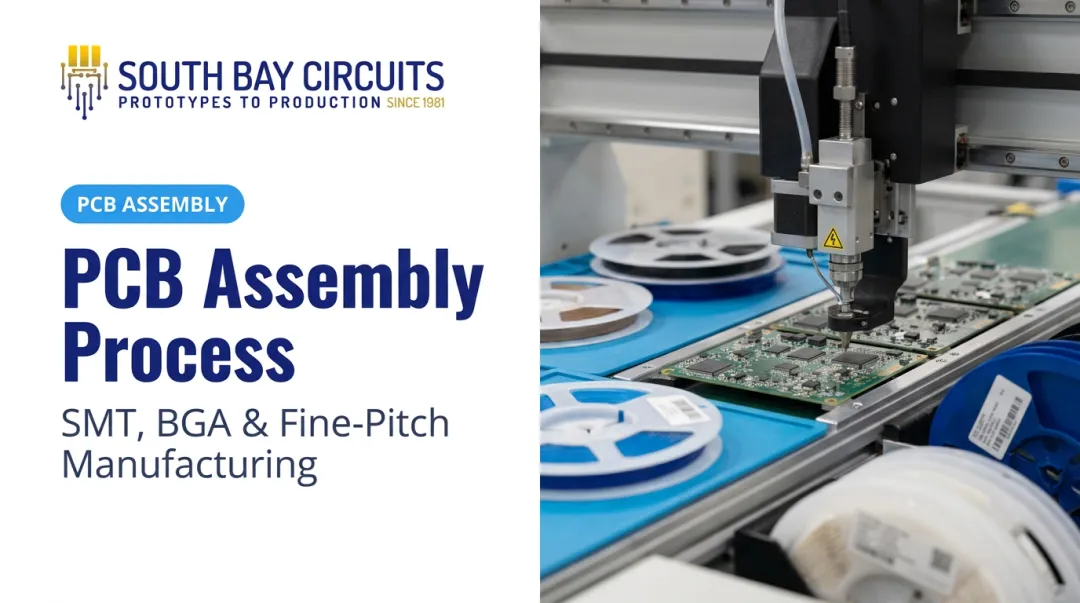
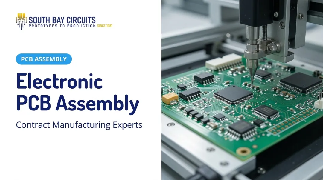
Pick-and-place machines mount resistors, capacitors, ICs, and other surface-mount devices onto the pasted pads. Vision-guided robotic placement does this at high speed and high precision. SBC runs Fuji SMT placement equipment, including chipshooters and flexible placers, and supports standard components down to 0201 package size and fine-pitch work down to 0.4mm with engineering review.
Step 3 — Reflow Soldering
The board then passes through a reflow oven running a controlled profile: preheat, soak, reflow, cool. According to Indium's reflow process guide, each phase has a distinct job:
- Preheat removes flux volatiles and reduces thermal shock
- Soak activates flux and equalizes temperature across the board
- Reflow melts the paste at peak temperature
- Cooling locks in the solidified joint structure
Get any phase wrong and you risk tombstoning, voiding, or cold joints.
Step 4 — Through-Hole Insertion and Wave/Selective Soldering
Components that need mechanical strength (connectors, transformers, larger passives) go through drilled holes rather than surface mounts. Depending on volume and part sensitivity, the line uses wave soldering, selective soldering, or hand soldering. Mixed-technology boards (SMT plus through-hole) are common on a single assembly.
Step 5 — Automated Inspection and Functional Testing
Before a board moves forward, several inspection layers check for defects:
- AOI catches missing components, wrong parts, polarity errors, and visible solder issues
- X-ray exposes hidden problems under BGAs and other area-array packages: voids, insufficient fill, head-in-pillow defects
- Flying probe or in-circuit testing verifies electrical continuity, resistance, capacitance, and shorts/opens
Step 6 — Cleaning, Coating, and Final Quality Checks
The line cleans off flux residue, often with a closed-loop deionized water system. Boards may receive conformal coating (silicone, acrylic, or urethane) for environmental protection in harsh-use applications. A final inspection confirms the board is ready to ship or integrate into a finished product.
Where the Process Is Applied and What Affects Its Output
Where the PCB Assembly Line Is Used
The same line supports a wide range of workflows, not just high-volume mass production:
- Prototype runs and new product introduction (NPI)
- Pilot runs to validate a design before scaling
- Full-scale production
- Rework and repair cycles for existing designs
That same process runs again at multiple points in a product's life: every new design release, every volume ramp-up, and every component or design change that forces a re-run.
Key Factors That Affect Line Performance
Several variables determine how a line gets configured for a given job:
- BOM quality and packaging — tape/reel or tray packaging affects placement accuracy and throughput; a messy BOM slows everything down
- Board complexity — layer count, component density, and fine-pitch parts change cycle time and how much inspection is warranted
- Regulatory constraints — ITAR registration, AS 9100, or medical-grade requirements add documentation, traceability, and testing steps on top of the same physical process
On the inspection side, complexity matters more than volume. According to Viscom's technical documentation on X-ray inspection, miniaturization and higher packing density push more connections into an assembly's interior. BGAs, flip chips, and internal voids increasingly need X-ray rather than optical inspection alone.
For defense-related work specifically, ITAR registration under 22 CFR 122.1 applies when a company manufactures, exports, or furnishes services related to defense articles. That adds recordkeeping obligations on top of standard IPC workmanship documentation.
South Bay Circuits' ITAR registration and CMMC Level 1 compliance support this kind of defense-program work, with component and process traceability through its ERP system.
Common Issues and When a Full Assembly Line Isn't the Right Fit
Common Issues and Misconceptions
The biggest misconception: treating "PCB assembly" as one uniform step instead of a multi-stage process with distinct checkpoints. Each stage (printing, placement, soldering, inspection) has its own failure modes and quality gate.
A related mistake shows up on small runs: skipping AOI or X-ray inspection to save time or cost. That gamble raises the risk of field failures later, since hidden BGA joint issues stay invisible regardless of run size. Low volume doesn't shrink defect risk; it only shrinks the sample size.
When the Full Line May Not Be Appropriate
A full automated line isn't always the right tool:
- Single-unit prototypes are often faster and cheaper with manual or semi-automated assembly
- Designs that change weekly rarely justify full SMT line setup time
- Early NPI builds may need process flexibility more than line throughput
- Very low annual volumes can make high-volume line programming a poor cost fit
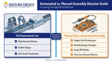
If a bench technician could build a one-off faster and cheaper than programming a high-volume line, the process is over-engineered for the job. Match the assembly method to volume and change rate, not to the equipment you happen to have.
Conclusion
The PCB assembly line process is a multi-stage, quality-controlled sequence, not a single step, that turns a bare board into a functional, tested assembly. Understanding each stage, from paste application through final inspection, directly affects cost, timeline, and compliance risk—especially in medical, aerospace, and automotive work.
What matters next is matching the right process and partner to your volume, complexity, and industry requirements. A single-source manufacturer like South Bay Circuits, which controls fabrication through assembly under one roof in its Chandler, Arizona facility, reduces handoffs and keeps accountability clear so you can choose on fit—not on whoever has the most complex line or the next open slot.
Frequently Asked Questions
What is PCB assembly (PCBA)?
PCBA stands for printed circuit board assembly—the process of placing and soldering electronic components onto a bare board to create a functional circuit.
Is PCB assembly expensive?
Cost varies based on board complexity, component count, volume, and compliance needs. Consolidating fabrication and assembly with one manufacturer often reduces total cost versus coordinating separate vendors.
What is the difference between PCB fabrication and PCB assembly?
Fabrication creates the bare board through etching, drilling, and laminating. Assembly mounts and solders components onto that finished board to make it functional.
How long does a typical PCB assembly line run take?
Timing depends on board complexity and volume, from a few hours for small prototype runs to continuous multi-shift schedules for high-volume production.
What is the difference between SMT and through-hole assembly?
SMT mounts components directly on the board surface, favoring speed and density. Through-hole inserts leaded components into drilled holes, favoring mechanical strength.
What certifications matter most for PCB assembly in regulated industries?
ISO 9001 covers general quality management. ISO 13485 addresses medical device reliability, AS 9100 covers aerospace/defense traceability, and IATF 16949 (ISO/TS 16949) addresses automotive durability requirements.