IPC's 2022 electronics-assembly benchmark found that rework and scrap costs, measured as a share of cost of goods, increased industry-wide — a signal that undetected defects are getting more expensive to fix downstream. That's exactly the gap flying probe testing (FPT) closes.
FPT gives engineers a fixtureless way to verify electrical integrity before a board ships, without waiting weeks for custom tooling. This guide breaks down how it works, when it makes sense, and what to expect from the process.
TL;DR
- Flying probe testing (FPT) is a fixtureless, software-driven method ideal for prototypes and low-to-mid volume PCB assemblies
- Movable probes check opens, shorts, resistance, capacitance, and polarity without a custom bed-of-nails fixture
- Delivers lower upfront cost, faster programming, and better access to dense, fine-pitch boards
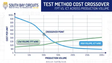
- High-volume production still favors in-circuit testing (ICT) for speed and lower per-unit cost
What Is Flying Probe Testing?
Flying probe testing is a PCB inspection method that uses movable, software-guided probes to check electrical connections and component values. No custom fixture is required. It's used across quality control, new product introduction (NPI), and low-volume production runs where board designs change frequently.
Traditional ICT relies on a bed-of-nails fixture: a custom-built plate with spring-loaded pogo pins aligned to a specific board's test points. Every design revision means building a new fixture. FPT skips that step entirely, using probes that reposition themselves based on the test program.
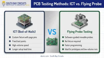
Keysight's 2025 comparison of ICT and flying probe testing notes that FPT programs can be generated straight from PCB design files, cutting out mechanical fixture fabrication. That's a meaningful advantage when a board might see three or four revisions before it's locked for production.
FPT can be applied to bare boards during fabrication or to fully assembled PCBs (sometimes called fixtureless in-circuit test, or FICT), depending on what stage of the build needs verification.
What Equipment Is Used for Flying Probe Testing?
A flying probe system has three core components:
- Probes — pogo pins for continuity, active probes for high-frequency or sensitive measurements, Kelvin probes for precise low-resistance readings
- Test fixtures — typically a generic board holder rather than a board-specific tool
- Control software — builds the test program from CAD data (ODB++ or IPC-2581) and a BOM, optimizes probe paths, and outputs pass/fail reports
Many systems also include cameras for automated polarity and orientation checks, using board fiducials for micron-level alignment. Board size and component height limits vary by model. Some testers handle boards over a meter long; others are built for smaller, denser assemblies.
What Types of Flying Probe Systems Exist?
System configuration depends on the boards being tested:
- Single-sided systems work well for simpler, lower-volume boards where all test points sit on one side
- Double-sided systems access both sides simultaneously, better suited to complex multilayer boards with components on top and bottom
- Multi-probe, high-speed configurations add extra probe heads to cut cycle time for medium-volume runs
Choosing between them comes down to board complexity, expected volume, and how tight the electrical tolerances are.
Why Flying Probe Testing Is Critical for PCB Assembly
FPT reduces risk earlier in the build process, which translates directly into faster NPI cycles and higher first-pass yield once a design moves toward production.
Here's why it matters:
- Cost-effective for prototypes and small batches — no custom fixture means lower upfront spend, especially valuable when a design might still change
- Better accessibility — reaches fine-pitch pads, microvias, and densely populated boards more easily than fixture-based testing
- Design flexibility — updating a test program is a software task, not a hardware rebuild
- Broader test coverage — probes access component pins and test points directly rather than through a fixed pattern
- Lower mechanical stress — reduces damage risk on thin or sensitive boards during test
Volume matters too. SPEA's 2025 comparison of the two methods states that bed-of-nails ICT tends to make sense above roughly 100,000 boards per year, while FPT better serves lower volumes and designs that change often.
Below that threshold, the fixture investment for ICT rarely pays for itself before the design revs again.
Lead time is another practical advantage. A custom ICT fixture for a complex board can take several days to build. FPT programming, by contrast, runs directly off CAD production data — no fabrication queue, no waiting on tooling.
How Flying Probe Testing Works – Step by Step
Here's how an assembly house typically moves a board through FPT, from program setup to defect reporting.
One early snag to watch: incomplete CAD or BOM data, or skipped test point verification, can delay the process or produce inaccurate results before testing even begins.
Step 1 – Create the Test Program
The test program is built from CAD production data (ODB++ or IPC-2581) combined with the bill of materials. This mapping identifies every net, pad, and via that needs to be tested.
Step 2 – Load and Calibrate
The board goes onto a conveyor or fixture bed. Probes and cameras calibrate against board fiducials for micron-level alignment before any measurement begins.
Step 3 – Run the Test
Probes contact component pads, test pads, and unmasked vias, applying electrical signals to measure resistance, capacitance, continuity, and polarity across the mapped nets.
Step 4 – Analyze and Report Results
The system compares measured values against expected tolerances. It flags anything outside spec and generates a pass/fail report with defect location data attached.
Step 5 – Review and Act on Findings
Flagged defects feed back into rework decisions, design revisions, or DFM discussions so the same issue does not reappear on the next build.
Example Walkthrough: Testing a Prototype PCB
Picture a new prototype board moving through its first FPT cycle. The program is generated from the CAD files, the board loads, probes calibrate, and testing begins. Partway through, the system flags a solder-related fault on one net.
On review, the outcome looks like this:
- Root cause: insufficient test pad clearance on a densely packed section
- Effect: the probe could not make consistent contact
- Action: design team adjusts pad spacing before full production
- Payoff: one early flag avoids a much costlier fix after shipment
How South Bay Circuits Can Help
South Bay Circuits (SBC) builds flying probe testing into its fabrication and assembly workflow rather than outsourcing it to a separate test house. That single-source setup cuts hand-offs and extra shipping, with one point of accountability for the whole build.
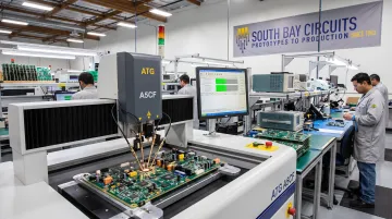
SBC runs an ATG A5CF Flying Probe Test System as part of its final electrical testing process, verifying circuit continuity and flagging potential faults before boards move forward.
Depending on the board type, SBC also applies bed-of-nails fixtures for single-sided testing or clamshell fixtures for double-sided SMT boards, matching the test method to the assembly.
What this means for customers:
- Fits testing inside SBC's quick-turn workflow, including 24-hour PCB fabrication and same-day assembly options
- Aligns quality processes with ISO 9001:2015, AS9100 (aerospace), ISO 13485 (medical), and ISO/TS 16949 (automotive) requirements
- Keeps design, fabrication, assembly, and test under one roof at the 60,000+ sq. ft. Chandler, Arizona facility
- Brings four decades of manufacturing experience to defense, medical, and other high-reliability programs
Conclusion
Flying probe testing gives engineering teams a practical way to validate PCB assemblies without the cost and lead time of a custom fixture. It is best suited to prototypes and low-to-mid volume builds. High-volume production still leans on ICT for speed at scale.
Test strategy works best when it's planned early in the design cycle, not bolted on afterward, and revisited as the board evolves. If you're weighing FPT for an upcoming build, SBC's team can walk through how it fits your project. Reach out at sales@sbcinc.com or +1 480-940-3125.
Frequently Asked Questions
What is flying probe testing?
Flying probe testing is a fixtureless PCB testing method that uses movable, software-guided probes to check electrical connections, component values, and defects. It skips the custom fixture that traditional in-circuit testing requires.
What equipment is used for flying probe testing?
Systems rely on three core components: probes (spring-loaded, active, or Kelvin types), a generic test fixture or board holder, and control software that generates test programs and analyzes results.
How does flying probe testing differ from in-circuit testing (ICT)?
ICT uses a custom bed-of-nails fixture built for one specific board, favoring speed at high volume. FPT uses software-guided probes with no fixture, favoring flexibility for prototypes and low-volume runs.
Is flying probe testing suitable for high-volume production?
Usually not. FPT works best at low-to-mid volumes since ICT offers faster per-unit cycle times once production scales into the hundreds of thousands of units annually.
What defects can flying probe testing detect?
FPT catches opens, shorts, incorrect component values, and polarity errors. More advanced testing can also identify micro-shorts and high-resistance faults.
How does the cost of flying probe testing compare to ICT?
FPT has a lower upfront cost since there's no fixture to build, but a higher per-unit cost due to longer sequential test cycles. ICT flips that: higher upfront investment, lower cost per unit once running.