Introduction
Getting from circuit concept to production-ready board involves far more than drawing a schematic and sending files to a fabricator. Every phase of the PCB design and prototyping process carries real consequences for quality, schedule, and cost — and skipping steps rarely saves time.
This guide is written for electronics engineers, hardware developers, and procurement managers in industries where design failures are expensive. In aerospace, medical, automotive, and defense applications, a missed DFM issue or skipped validation step can trigger regulatory non-compliance, production rework, or field failures that no schedule pressure justifies.
According to IPC's rigid-PCBA process checklist, the complete design-to-production workflow spans 32 parameters and 212 variables — each representing a potential failure point if the process isn't followed with discipline.
This article walks through every phase: design, fabrication, assembly, testing, and the factors that determine whether your prototype actually reflects your final product.
Key Takeaways
- PCB prototyping is where design flaws, DFM conflicts, and performance gaps get caught and resolved before volume production begins.
- The process spans five distinct phases: schematic capture, layout and file generation, fabrication, assembly, and testing/validation.
- DFM readiness, material selection, and parts kit completeness are the variables most within your control when managing prototype turnaround.
- High-stakes industries (aerospace, medical, defense, automotive) require strict compliance with standards like AS9100D, ISO 13485, and IATF 16949.
- A single-source manufacturer covering design through loaded assembly cuts iteration time by removing vendor handoff delays.
What Is the PCB Design and Prototyping Process?
The PCB design and prototyping process is the end-to-end workflow that begins with circuit schematic design and ends with a functionally tested, assembled board. Every stage is validated against specifications before any commitment to full-scale production.
The goal isn't just a working board. It's a manufacturable board that performs reliably in its intended environment, produced in a small representative quantity for testing and approval.
Prototyping vs. Production: Key Differences
These two stages share the same fabrication and assembly processes, but they differ in intent and execution:
| Factor | Prototyping | Production |
|---|---|---|
| Quantity | Low (typically 1–10 units) | High volume |
| Priority | Design flexibility, iteration speed | Yield, cost, repeatability |
| Tolerance | Exploratory | Locked and verified |
| Goal | Validate design | Execute proven design |
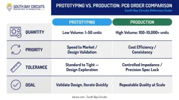
The distinction matters because decisions made during prototyping — stackup choices, component placement, design rule tolerances — carry directly into production. Getting them right early is far cheaper than correcting them at volume.
Key reasons teams invest in a structured prototyping phase:
- Catches design errors before tooling and materials are committed at scale
- Validates electrical performance, thermal behavior, and mechanical fit in real conditions
- Produces documented evidence of design intent for regulatory or customer approval
- Enables DFM feedback from the fabricator before production quantities are ordered
How the PCB Design and Prototyping Process Works
At a high level: a designer creates a schematic, develops a physical layout, generates manufacturing files, sends them to a fabricator who builds the bare board, an assembler places and solders components, and the finished board undergoes electrical and functional testing. If issues are found, the design iterates before production approval.
Here's how each stage works in practice.
Step 1: Schematic Capture and Component Selection
Schematic capture converts circuit logic into symbolic diagrams using EDA tools such as Altium Designer, KiCad, or Eagle. Each component — resistor, capacitor, IC — is placed and connected to represent the electrical relationships in the design.
Component selection at this stage must account for:
- Electrical specifications (voltage ratings, tolerances, frequency response)
- Footprint compatibility with the planned PCB layout
- Availability and lead time — components that look good on paper but are on allocation will stall assembly
- Cost within BOM targets
A Bill of Materials (BOM) is generated here and follows the design through every subsequent stage. Errors introduced in the BOM at this point — wrong part numbers, incorrect quantities, mismatched footprints — are among the most common causes of assembly delays and rework.
Step 2: PCB Layout, Design Rule Check, and File Generation
The schematic is transferred into a physical board layout where traces are routed, layers are defined, and component placement is optimized for signal integrity and thermal management.
Before files leave the design environment, a Design Rule Check (DRC) is run to catch:
- Spacing and clearance violations
- Copper-to-edge proximity issues
- Connectivity errors (unconnected nets, shorts)
- Footprint mismatches against the schematic
DFM (Design for Manufacturability) analysis runs alongside DRC to flag issues that would complicate or prevent fabrication — trace widths below process minimums, annular ring violations, or soldermask slivers that a fab can't reliably produce.
Once DRC and DFM review pass, Gerber files (RS-274X format) and NC drill files are exported for the fabricator. Incomplete or inconsistent file packages are the single most common reason pre-production reviews stall before the fabrication clock starts.
Step 3: PCB Fabrication
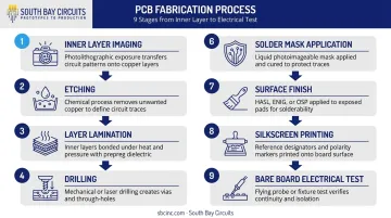
Bare board fabrication follows a defined sequence, and each sub-step must execute within tight tolerances or the board fails downstream:
- Inner layer imaging — photolithography exposes copper patterns on each layer
- Etching — unwanted copper is chemically removed
- Layer lamination — layers are pressed together under heat and pressure
- Drilling — mechanical or laser drilling creates via and through-hole openings
- Copper plating — via walls are plated to establish electrical continuity between layers
- Solder mask application — LPI coating protects copper and defines pad openings
- Surface finish — HASL, ENIG, OSP, or immersion silver applied per design requirements
- Silkscreen printing — reference designators and assembly markings applied
- Bare board electrical test — continuity and isolation verified; open/short testing per IPC-9252B confirms every net before boards ship
Material selection directly affects this sequence. Standard FR-4 (such as Isola IS410 with a 180°C Tg) processes differently than Rogers RO4000 series laminates used in microwave and millimeter-wave applications — which require dedicated drilling, lamination, and handling procedures per Rogers' published fabrication guidelines.
Step 4: PCB Assembly
Assembly converts a bare board into a functional unit. The standard SMT sequence:
- Solder paste stenciling — automated screen printer deposits paste onto pads
- Pick-and-place — automated equipment mounts SMD components with precision
- Reflow soldering — convection oven cures paste and forms solder joints
- Wave or hand soldering — through-hole components soldered after SMT reflow
- Cleaning — flux residue removed per process requirements
Two-sided boards require separate stencil and reflow passes per side, adding time and complexity. Parts kit completeness is critical here: the assembly clock doesn't start until all components are inventoried and checked in. A single back-ordered part holds the entire board.
South Bay Circuits addresses this directly: component sourcing runs concurrently with bare board fabrication at their Chandler, AZ facility, so procurement doesn't become the bottleneck once boards come off the line.
Step 5: Testing, Validation, and Design Iteration
Once assembled, boards move through a structured inspection and test sequence before any production approval:
- AOI (Automated Optical Inspection) — verifies component placement and solder joint quality against IPC-A-610 acceptance criteria
- X-ray inspection — examines hidden solder joints (BGAs, buried vias) per IPC-7095 methods
- Electrical and functional testing — validates board performance against operating specifications
- ICT (In-Circuit Test) — probes assembled nodes to verify component values and connectivity
Test failures trigger a design iteration loop: schematic or layout revisions, new Gerber generation, re-fabrication, and re-assembly. Designs that skip pre-layout simulation typically require two to three prototype spins; those with thorough pre-layout analysis often close in one.
Working with a single-source partner like South Bay Circuits (which handles design through loaded assembly under one roof) compresses this iteration cycle by eliminating queue time and communication gaps between separate vendors. Their in-house capabilities include Glenbrook X-ray inspection, AOI, ICT, functional testing, burn-in testing, and Polar TDR impedance testing — all applied within the same production run.
Why the PCB Design and Prototyping Process Matters in High-Stakes Industries
In aerospace, defense, medical, and automotive applications, a design defect discovered post-production carries consequences well beyond rework costs — recalls, regulatory action, and field failures in life-critical systems.
Regulatory Standards Governing PCB Quality
These industries operate under formal quality management systems that impose design, manufacturing, and traceability requirements at every stage:
| Industry | Standard | Scope |
|---|---|---|
| Aerospace / Defense | AS9100D | Organization-level QMS for aviation, space, and defense |
| Medical Devices | ISO 13485:2016 | QMS requirements for medical device manufacturers |
| Automotive | IATF 16949:2016 | Automotive QMS; replaced ISO/TS 16949:2009 |
| High-Reliability Boards | IPC-6012 Class 3 | Qualification/performance for harsh-environment PCBs |
| Defense PCBs | MIL-PRF-31032 | U.S. DoD rigid PCB performance specification |
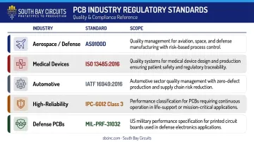
South Bay Circuits holds compliance with IPC-6012 Class III, MIL-PRF-31032, MIL-PRF-55110, and ITAR registration, and operates under AS9100, ISO 13485, and IATF 16949-aligned quality systems with CMMC Level 1 compliance. That credential set covers all four sectors above.
What Goes Wrong Without Prototyping
Skipping or shortcutting validation in regulated industries produces predictable failure modes:
- Signal integrity failures that only appear under operating conditions
- Thermal management gaps where component self-heating exceeds design assumptions
- Component misalignment that passes visual inspection but fails under vibration or thermal cycling
- Board-level reliability failures that surface in the field rather than in development
The FDA's device recall records include power-management PCBA failures in life-critical ventilator equipment — a real-world example of what happens when board-level validation is insufficient before deployment.
The Prototype-to-Production Transition
This is the moment where DFM alignment, manufacturing tolerances, and quality systems must be locked in. Switching manufacturers between prototype and production resets qualification entirely. Even minor material changes can shift thermal performance or signal integrity outside validated parameters.
A contract manufacturer that built the prototype and can scale production without re-qualification removes a significant NPI risk. The design is already characterized on the same equipment, in the same facility, under the same quality system — so the re-qualification overhead that fragmented supply chains require simply doesn't apply.
Key Factors That Affect PCB Prototype Quality and Turnaround
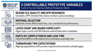
Most prototype delays trace back to a small set of controllable variables:
Design file quality and DFM readiness — incomplete Gerber packages, missing drill files, or undefined stack-up requirements trigger pre-production delays. The CAM review doesn't start the fabrication clock until these are resolved — submitting a complete, reviewed file package is the highest-leverage action a design team controls.
Material selection — FR-4 processes quickly and is widely available. Rogers RO4000 laminates for high-frequency designs require dedicated handling per supplier fabrication guidelines. Polyimide and other specialty substrates require additional process controls. Non-standard materials extend prototype lead times, sometimes by a week or more.
Layer count and board complexity — additional layers mean more lamination cycles, more registration controls, and more opportunities for yield loss. Blind/buried vias, controlled impedance routing, and fine-pitch components all require advanced fabrication capabilities. Confirm your manufacturer's process limits before submitting files.
Parts kit completeness and lead time — IPC's February 2025 global EMS survey found 50% of electronics manufacturers facing rising material costs and tightening component availability. Components ordered late, back-ordered, or shipped in split consignments consistently delay assembly — the clock doesn't start until all parts are checked in.
Turnaround time expectations vs. actual process requirements — a 24-hour fabrication claim only holds if DFM review is already complete. Factor pre-production engineering time into your schedule: bare board lead times run 24 hours for simple, DFM-clean designs up to 2–3 weeks for complex multilayer boards with specialty substrates or advanced via structures.
Common Misconceptions About PCB Design and Prototyping
"Minor changes don't need prototyping"
Any modification to trace routing, layer stack-up, component footprint, or substrate material changes how the board behaves electrically and mechanically. Even incremental changes can introduce unexpected signal integrity failures, impedance drift, or assembly issues.
Treating a small change as low-risk is a reliable way to learn otherwise — after committing to production volume.
"Fast fabrication means production-ready"
Rapid fabrication reduces bare board turn time. It doesn't substitute for DRC review, DFM analysis, or functional testing. Teams that equate fabrication speed with design readiness often discover errors only after committing to production quantities, when rework costs have already outgrown prototype scale.
"We can skip prototyping to hit schedule"
Skipping prototyping is only appropriate in one narrow scenario: re-running an exact, previously validated design with the same manufacturer, same materials, and same components in the same application environment. Any of the following resets that exception:
- New manufacturer or fabrication facility
- Component substitution, even pin-compatible parts
- Design revision of any scope
- New application environment or end-use context
Schedule pressure drives most decisions to skip validation. It also drives most post-production rework events.
Conclusion
The PCB design and prototyping process converts a circuit concept into a validated, manufacturable board by moving through a defined sequence — design, fabrication, assembly, and testing — where each stage builds on the one before it.
For teams working in aerospace, defense, medical, and automotive applications, this process is a reliability and compliance requirement, not an optional best practice. Investing in proper prototyping — with a single-source manufacturer that handles design through loaded assembly — reduces NPI cycle times, avoids production rework, and produces more predictable end products.
That kind of single-source capability is what South Bay Circuits has delivered since 1981. From its 60,000 sq ft Chandler, AZ facility, SBC manages the full process — design, fabrication, and loaded assembly — under one roof, with the compliance credentials to support regulated industries:
- IPC-6012 Class III / MIL-PRF-31032 for military and high-reliability boards
- AS9100 and ITAR registration for aerospace and defense programs
- ISO 13485 for medical device electronics
- ISO TS 16949 for automotive applications
- ISO 9001:2015 as the quality management baseline across all programs
Whether you're moving a design from prototype to production or compressing NPI timelines on a regulated program, SBC's single-source model eliminates handoff delays, reduces rework risk, and keeps the entire process accountable under one contract.
Frequently Asked Questions
What is PCB prototyping?
PCB prototyping is the process of fabricating and assembling a small quantity of boards from a new design to test functionality, verify manufacturability, and identify design issues before committing to full production volume. It is the primary mechanism for resolving design, DFM, and performance gaps at low cost.
How long does PCB prototyping take?
Prototype timelines range from 24 hours for simple, DFM-ready designs to several weeks for complex multilayer boards with specialty substrates or advanced via structures. The pre-production DFM review must complete before fabrication begins, so lead time is not purely a function of manufacturing speed.
What is the difference between PCB fabrication and PCB assembly?
Fabrication builds the bare board — substrate, copper layers, vias, solder mask, and surface finish. Assembly places and solders components onto that fabricated board. Both stages are required to produce a functional PCB, and they involve different processes, equipment, and quality standards.
What files are needed to start the PCB prototyping process?
The standard package includes:
- Gerber files (RS-274X format) for each layer
- NC Excellon drill file and drill tool list
- Bill of materials (BOM)
- Assembly drawings or special notes
Incomplete or mismatched files are the most common cause of pre-production delays. The CAM review cannot begin until the package is complete.
How many prototype iterations are typically needed before production?
Simple designs may resolve in one or two spins. Complex multilayer, high-frequency, or safety-critical boards often require three or more iterations before the design is stable enough for production approval. Pre-fabrication simulation rigor is the main variable that reduces spin count.
When can a design go straight to production without prototyping?
Only when re-running an exact, previously validated design with the same manufacturer, materials, and components in the same application. Any design change, supplier change, component substitution, or new application environment warrants a prototype validation step before committing to production volume.