Introduction
PCBs are inside virtually every electronic device you interact with daily — your smartphone, the medical monitor in a hospital room, the radar system aboard a military aircraft, and the power management unit in an electric vehicle. They're everywhere, yet most people outside of engineering couldn't explain what one actually is.
A printed circuit board is a structured platform that mechanically supports and electrically connects electronic components using conductive copper pathways etched onto a non-conductive substrate. In plain terms: it's the backbone of nearly all modern electronics.
This guide covers:
- What a PCB is and how it works
- Materials and construction methods
- Types of PCBs and their applications
- The manufacturing process from design to finished board
- Where PCBs are used across industrial, medical, aerospace, automotive, and defense applications
Written for engineers, procurement managers, and product developers evaluating PCB solutions at any production scale.
Key Takeaways
- A PCB is a laminated board of conductive and insulating layers that mechanically holds and electrically connects electronic components
- PCBs come in several types — single-sided, double-sided, multilayer, rigid, flexible, and rigid-flex — each suited to different performance requirements
- Manufacturing spans design, fabrication, and assembly — SMT and THT are the two primary assembly methods
- High-reliability industries like aerospace, medical, and defense require specific certifications and fast turnaround
What Is a PCB and How Does It Work?
A printed circuit board is a flat board — rigid or flexible — made of insulating substrate material with layers of conductive copper traces etched onto or between them. It mechanically supports and electrically connects the components that make a device function.
The word "printed" refers to the manufacturing process: conductive pathways are chemically etched or deposited onto the board using photographic and chemical processes — not hand-drawn. This distinguishes modern PCBs from the point-to-point wired assemblies of early electronics, which were bulky, unreliable, and impossible to mass-produce consistently.
How Current Flows Through a PCB
When power is applied, electric current travels through the copper traces, routing signals and power between:
- Active components — transistors, integrated circuits (ICs), diodes
- Passive components — resistors, capacitors, inductors
Together, these components and their interconnections allow a device to perform its intended function, whether that's amplifying a signal, storing data, or regulating voltage.
PCB vs. PCBA — A Common Source of Confusion
These two terms get used interchangeably, but they're not the same thing:
- PCB — the bare board: substrate, copper traces, pads, and protective layers, with no components attached
- PCBA (Printed Circuit Board Assembly) — the finished board with all electronic components soldered in place, ready to be integrated into a product
The distinction matters when quoting, specifying, or evaluating suppliers. A PCB manufacturer and a PCBA manufacturer may be the same company — or two separate vendors.
The Scale of the Industry
That distinction — PCB vs. PCBA — plays out across an industry of significant size. The global PCB market was valued at USD 82.7 billion in 2025, with Grand View Research projecting a 5.8% CAGR through 2033, reaching USD 130.3 billion by that point. The growth reflects demand from every electronics-dependent sector: defense systems, medical devices, automotive platforms, and consumer tech alike — all built on the same fundamental component.
Key Components of a Printed Circuit Board
Every PCB is built from several distinct physical layers, each with a specific role. Knowing what each layer does — and why it was chosen — is what separates a board spec that works from one that causes problems in fabrication or the field.
Substrate and Insulating Layers
The substrate forms the structural foundation. It provides insulation between conductive layers, mechanical rigidity, and resistance to heat and moisture.
The most common substrate is FR-4 — a flame-retardant, woven fiberglass and epoxy resin laminate that balances performance, manufacturability, and cost. Other substrate options include:
- Polyimide — used for flexible PCBs; offers flexural endurance and low weight
- Metal-core (MCPCB) — aluminum or copper-backed construction that spreads heat away from high-power components
- Ceramic — used in high-frequency or extreme-temperature applications where standard epoxy laminates fall short
Substrate selection isn't cosmetic. It directly affects thermal performance, signal integrity, and long-term reliability — and it shapes every conductive layer built on top of it.
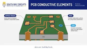
Copper Traces, Pads, and Vias
These are the conductive elements that make the board functional:
- Copper traces — thin, flat pathways etched from copper foil that carry signals or power between circuit nodes, functioning like wires embedded in the board
- Pads — flat copper surfaces where component leads are soldered, providing the mechanical and electrical connection point
- Vias — metal-plated holes that allow electrical connections to pass between different copper layers in multilayer boards; essential for routing in complex designs
Solder Mask and Silkscreen
Two finishing layers that protect the board and support assembly:
- Solder mask — a polymer coating (typically green, though blue, red, and black are common) applied over copper traces to prevent oxidation, short circuits, and solder bridges during assembly; pads and vias remain exposed for soldering
- Silkscreen — the printed text, symbols, and reference designators on the board surface identifying component placement, polarity, and board markings. Essential during assembly and field repair.
Types of PCBs Explained
PCBs are classified in two ways: by the number of copper layers and by the flexibility of the substrate.
Classification by Layer Count
| Type | Description | Typical Use |
|---|---|---|
| Single-sided | One copper layer; simplest construction | Basic consumer electronics, simple sensors |
| Double-sided | Copper on both sides, connected by vias | More complex circuits, industrial controls |
| Multilayer | Three or more layers laminated together | High-density designs, advanced electronics |
Multilayer boards are where design complexity increases. Four layers is a common entry point for signal and power plane designs — handling protocols like USB, HDMI, and Ethernet. Complex applications can push well beyond that, with some boards reaching 16 or more layers to achieve component density in a compact footprint.
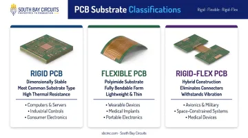
Classification by Substrate Flexibility
- Rigid PCBs — the most common type, used in computers, industrial equipment, and most consumer electronics. Dimensionally stable, relatively easy to manufacture.
- Flexible PCBs (flex) — made from polyimide; bend and fold to fit wearables, cameras, and medical devices where rigid boards won't work.
- Rigid-flex PCBs — combine rigid sections for component mounting with flexible sections for routing between them. Common in radar, avionics, and military electronics where space and weight are constrained.
Why Type Selection Matters
Both classification dimensions — layer count and substrate type — affect performance, reliability, and regulatory compliance in ways that are hard to reverse after fabrication begins. A wearable medical device may require flex construction to pass IEC 60601 testing. An avionics assembly might demand a multilayer rigid-flex to meet AS 9100 reliability standards in a constrained form factor. Locking in the right board type during design review avoids costly respins and schedule delays later.
How PCBs Are Designed and Manufactured
PCB manufacturing spans multiple stages — from schematic to shipped assembly — each with defined inputs, outputs, and inspection checkpoints.
The Design Phase
Engineers start with a schematic : a 2D circuit blueprint created in EDA software (Altium Designer, KiCad, or Cadence Allegro) that defines which components are used and how they connect. The schematic is then translated into a PCB layout: a physical arrangement specifying where each component sits and how traces are routed.
Good layout design accounts for:
- Signal integrity (minimizing noise and interference)
- Thermal management (preventing hotspots)
- DFM rules (design for manufacturability — ensuring the board can actually be built)
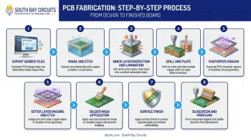
Fabrication Steps
Once the design is finalized, fabrication follows a defined sequence:
- Export Gerber files — the design is output as manufacturing data (Gerber or ODB++), including drill files, stackup, and layer artwork
- Image and etch — conductor patterns are imaged onto resist-coated copper laminate, developed, and unwanted copper is etched away
- Inner layer inspection and lamination — inner layers are inspected, stacked with prepreg (bonding material), and pressed together under heat and pressure
- Drill and plate — holes are drilled for vias and through-hole components, then plated to create electrical connections
- Outer layer imaging and etch — the same process is applied to external copper layers
- Solder mask application — polymer coating is applied and cured; pad openings are exposed
- Surface finish — exposed copper receives HASL (hot air solder leveling) or ENIG (electroless nickel immersion gold) to prevent oxidation and improve solderability
- Silkscreen and profiling — legends are printed, boards are routed to final dimensions, and electrical inspection is performed
Assembly Methods
Two primary techniques are used to attach components:
- SMT (Surface Mount Technology) — automated pick-and-place machines deposit solder paste on surface pads, position components, and the board passes through a reflow oven to complete the bond. Enables high-density, miniaturized designs.
- THT (Through-Hole Technology) — component leads pass through drilled holes and are soldered by wave or selective soldering. Provides greater mechanical strength, often used for connectors and high-power components.
Many boards use both methods in the same assembly.
Quality Control and Testing
High-reliability manufacturing programs define inspection at every stage, not just the end of line. A complete plan typically includes:
- AOI (Automated Optical Inspection) — detects visible defects: missing parts, solder bridges, polarity errors
- X-ray inspection — reveals hidden solder structures under packages like BGAs, where optical access is impossible
- ICT (In-Circuit Testing) — electrically probes board nodes to identify opens, shorts, and component faults
- Functional testing — powers the assembly and verifies actual input/output behavior
ISO 9001:2015 certification signals that a manufacturer has established quality management processes covering controlled production, records, corrective action, and continual improvement — a baseline requirement for regulated-industry procurement. South Bay Circuits holds ISO 9001:2015, ITAR, and CMMC Level 1 credentials — and operates all stages of this process, from design through assembly, within its 60,000 sq ft Chandler, Arizona facility, with bare board fabrication available in 24 hours and 3-Day Turn or Less assembly for qualifying programs.
PCB Applications Across Industries
PCBs underpin electronics across nearly every sector. IPC's industry reporting segments demand into automotive, defense and aerospace, high-end systems, and industrial and medical electronics.
High-Reliability Applications
Industries like aerospace, defense, and medical impose requirements well beyond standard commercial boards:
- Boards must withstand extreme temperatures, vibration, and shock
- Components require traceability documentation throughout the supply chain
- Manufacturers must hold industry-specific quality management certifications
SBC holds AS9100 for aerospace, ISO 13485 for medical devices, and ISO TS 16949 for automotive — certifications that directly satisfy the entry requirements for these regulated markets.
Prototype to Production
For defense and medical programs, those certification requirements don't disappear at the prototype stage — they apply across the entire development lifecycle. Keeping one manufacturer from NPI through production eliminates:
- Re-qualification of a new supplier
- Design translation errors between vendors
- Supply chain gaps during production ramp
SBC's integrated model covers prototype NPI through high-volume production, with offshore partnerships available for cost-optimized volume runs, so programs move forward without supplier transitions or qualification delays.
Common PCB Problems and Warning Signs
Even well-designed boards fail. Knowing what to look for speeds up diagnosis and reduces downtime.
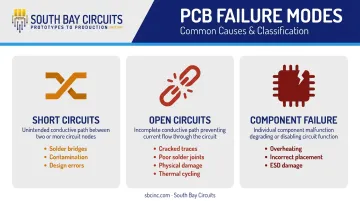
Primary Failure Modes
- Short circuits — unintended connections between traces from solder bridges, contamination, or design errors
- Open circuits — broken connections from cracked traces, poor solder joints, or physical damage; NASA documentation cites these as common failure mechanisms under thermal cycling or vibration
- Component failure — caused by overheating, incorrect placement, or ESD damage, which often leaves no visible mark and requires proper handling controls to catch
Visible Warning Signs
If you're inspecting a board that may be failing, look for:
- Burn marks or discoloration on the board surface
- Cracked or lifted traces
- Bulging or leaking capacitors
- Cold solder joints — dull, grainy appearance rather than smooth and shiny
- Intermittent device behavior or unexpected shutdowns
Diagnostic Methods
| Method | What It Finds |
|---|---|
| Visual inspection | Discoloration, damaged traces, solder bridges, physical damage |
| Multimeter (continuity) | Opens and unintended shorts between nodes |
| Thermal imaging | Abnormal hot or cold regions on a powered assembly |
| AOI (Automated Optical Inspection) | Repeated automated comparison for assembly anomalies |
Once you've identified the failure mode, the operating environment often explains why it occurred. Boards exposed to high heat, humidity, or vibration face higher failure rates than those running in controlled conditions. Applying conformal coating over the assembled board adds an electrically insulating protective layer that extends service life where conditions are most demanding.
Frequently Asked Questions
What does a circuit board do?
A circuit board mechanically supports all electronic components in a device and electrically connects them through copper traces, routing power and signals so the device can perform its intended function. Without it, components would have no structured way to communicate or share power.
How do I tell if my circuit board is bad?
Look for visible signs: burn marks, cracked traces, bulging capacitors, or dull/grainy solder joints. Device symptoms like failure to power on, random resets, or persistent overheating also suggest board-level faults. Multimeters and AOI systems can pinpoint specific failures more precisely.
How much does a circuit board cost?
Board cost depends on layer count, materials, surface finish, order quantity, and turnaround time. A simple single-sided prototype may run $50–$200 per board in small quantities, while complex multilayer designs can reach several hundred to thousands of dollars per unit at low volumes.
What is the difference between a PCB and a PCBA?
A PCB is the bare board — substrate, traces, and pads — with no components attached. A PCBA (Printed Circuit Board Assembly) is the completed board with all electronic components soldered in place, ready to be integrated into a finished product.
What materials are PCBs made of?
The most common substrate is FR-4 (woven fiberglass and epoxy resin). Copper forms the conductive traces, and a polymer solder mask protects them. Specialty applications may use polyimide (flexible PCBs), metal-core substrates (high-heat applications), or ceramic materials for high-frequency performance.
How many layers does a PCB typically have?
PCBs range from 1 layer (simple, low-cost applications) to 2, 4, 6, 8, or more. Four layers is a common entry point for multilayer designs handling protocols like USB or Ethernet. High-complexity devices — dense RF, server, or defense hardware — commonly reach 16 or more layers.