PCB potting is one of the most effective ways to stop that failure chain before it starts. Aerospace, medical, automotive, and industrial electronics manufacturers all rely on it to keep sensitive assemblies running in conditions that would otherwise destroy them.
This guide covers what potting actually means, the main compound types, the real benefits backed by engineering data, how potting compares to conformal coating, and what to look for in a manufacturing partner.
Key Takeaways
- Cured resin fully encapsulates the board, blocking moisture, vibration, and chemical exposure.
- Epoxy, silicone, and polyurethane solve different thermal, flexibility, and dielectric challenges.
- Compared to conformal coating, potting adds more thickness, weight, and permanence.
- Aerospace, medical, automotive, and industrial equipment rely on potting for long-term reliability.
- Planning potting during DFM review avoids costly redesigns and vendor handoffs later.
What Does Potting a Circuit Board Mean?
Potting means fully encapsulating an assembled board, or a specific component, inside a mold or housing filled with a liquid compound. That compound cures into a solid or gel-like mass that stays with the product permanently in most cases.
It's easy to confuse potting with encapsulation, but the two aren't identical:
| Aspect | Potting | Encapsulation |
|---|---|---|
| Coverage | Covers the whole assembly | Applies to a single component |
| Mold or housing | Often remains part of the finished product | Sometimes removed after cure |
Industry professionals frequently use the terms interchangeably, and IPC-HDBK-850, the handbook governing potting and encapsulation materials, acknowledges this overlap directly.
The Physical Process
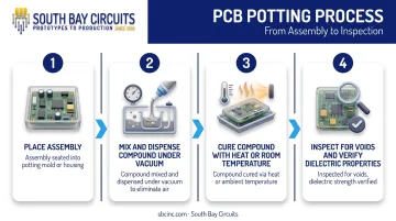
Potting follows a straightforward sequence:
- Place the assembly into a pot, mold, or housing designed to contain the liquid compound.
- Mix and dispense the compound, often under vacuum to remove trapped air.
- Cure the compound at room temperature or with applied heat, depending on the formulation.
- Inspect for voids and confirm dielectric and mechanical properties meet spec.
Getting this right requires more than pouring resin into a box. Engineers need to:
- Achieve void-free coverage throughout the encapsulant
- Match the compound's coefficient of thermal expansion (CTE) to the board and enclosure materials
- Confirm the cured mass meets dielectric requirements for the operating voltage
Miss any of these, and you trade one failure mode for another.
Potting differs from conformal coating mainly in thickness and coverage — a distinction that matters enough to warrant its own section later in this guide.
Key Benefits of PCB Potting for Electronic Assemblies
Potting solves several problems at once, which is exactly why reliability-critical industries lean on it so heavily.
- Environmental protection. Cured potting compound creates a physical barrier against moisture, dust, and corrosive chemicals. Boards exposed to humid or industrial environments without this barrier face a well-documented set of failure mechanisms, including delamination, reduced insulation resistance, and conductive filament formation as moisture works into resin and interfaces over time.
- Mechanical stability. The cured mass absorbs shock and vibration, protecting solder joints and fragile components. This matters most in transportation applications and industrial machinery, where constant vibration would otherwise fatigue connections over months of operation.
- Electrical insulation. Potting compounds provide dielectric strength that reduces short-circuit risk and corona discharge in high-voltage assemblies. Product-specific values vary widely, so the right number depends on the compound you select, not a generic epoxy or polyurethane average.
- Thermal management. Certain formulations are thermally conductive while remaining electrically insulating, helping pull heat away from sensitive components rather than trapping it.
- Tamper resistance. Ruggedized, opaque potting systems obscure components and make removal difficult without damaging the assembly, a real deterrent for defense electronics, cryptographic hardware, and proprietary circuit designs.
- Extended product lifespan. Combine all of the above, and you get fewer field failures and lower warranty exposure over the life of the product. That's why reliability-critical industries treat potting as standard practice rather than an optional add-on.
Types of PCB Potting Compounds
No single compound works for every application. Selecting the right one means balancing rigidity, temperature range, cure time, and cost against what the assembly actually needs to survive.
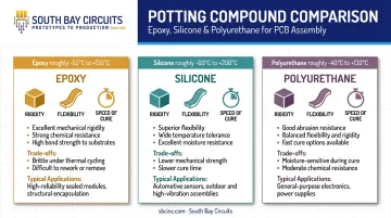
Epoxy Resin
Epoxy delivers rigidity, strong adhesion, and solid chemical resistance. It's a common choice for automotive electronics and power supply assemblies where mechanical strength matters most. The trade-off: epoxy typically holds up well within a -40°F to 250°F range, but repeated cycling beyond that spread causes brittleness, making it a poor fit for wide, frequent temperature swings.
Silicone
Silicone flexes rather than cracks, and it tolerates temperatures from about -65°F to 400°F, a range that suits aerospace and industrial environments where vibration and thermal extremes are constant. It generally trades some rigidity and mechanical strength for that flexibility.
Polyurethane
Polyurethane splits the difference: flexible enough to absorb impact, tough enough to resist tearing, and often curing in under an hour versus several hours for epoxy. That combination makes it a frequent choice for consumer electronics and LED drivers, where moderate protection and quick production cycles both matter.
Choosing the Right Compound
Match the compound to the application using these criteria:
- Dielectric strength needed for the operating voltage
- Thermal conductivity requirements for heat-sensitive components
- UV exposure if the assembly sees outdoor or sunlight conditions
- Reworkability if the design may need field service
- CTE matching to the board and enclosure materials to avoid stress cracking
| Compound | Strengths | Trade-offs | Typical Use |
|---|---|---|---|
| Epoxy | Rigid, strong adhesion, chemical resistant | Brittle under thermal cycling | Automotive, power supplies |
| Silicone | Flexible, wide temperature tolerance | Lower mechanical strength | Aerospace, vibration-heavy industrial |
| Polyurethane | Balanced flexibility and impact resistance, fast cure | Moderate chemical resistance | Consumer electronics, LED drivers |
PCB Potting vs. Conformal Coating: Which Protection Method Is Right for You?
Both methods protect boards, but they solve different problems. The core difference comes down to thickness.
Potting resin typically starts around 0.5 mm, while conformal coatings run 1-5 mils, or roughly 25-127 micrometers — a difference of an order of magnitude or more.
That thickness gap drives every other trade-off:
| Factor | Potting | Conformal Coating |
|---|---|---|
| Thickness | ~0.5 mm and up | 25-127 micrometers |
| Weight/volume | Adds significant mass and bulk | Minimal added weight |
| Protection level | Maximum, for harsh or extreme exposure | Moderate, for lighter exposure |
| Rework | Largely permanent once cured | Can be stripped and reworked |
Potting makes sense when the assembly faces extreme moisture, chemical exposure, or mechanical stress and space isn't a constraint. Conformal coating fits better in space- and weight-constrained products like handheld devices or wearables, where a thin barrier is enough and future rework matters.
Industries and Applications That Rely on PCB Potting
Potting shows up wherever electronics have to survive conditions that would otherwise take them out of service.
- Aerospace & defense: Avionics and flight-critical electronics endure extreme temperature swings and constant vibration throughout their service life; AS9100-compliant quality systems keep potting's process controls under the same scrutiny as the rest of the assembly.
- Medical devices: Life-critical electronics need resistance to contamination and mechanical failure across years of continuous operation; ISO 13485 compliance governs the traceability and process control that potting depends on.
- Automotive: Engine control units and sensors sit under the hood, exposed to heat, vibration, and fluid contact daily; potting shields these assemblies from the corrosion and solder-joint failures that would otherwise follow within a few years.
- Industrial and military equipment: Control panels and field electronics face dust, chemicals, and rough handling in demanding operating environments; potting keeps these systems running in conditions that would otherwise degrade an unprotected board quickly.
Choosing a Manufacturing Partner for PCB Potting Services
Potting works best when it's planned early, not bolted on after the board is already built. Bringing it into the DFM review means the compound, mold geometry, and cure process get designed alongside the board itself, not around it.
That's where a single-source manufacturer has a real advantage. Coordinating fabrication, assembly, and potting across separate vendors adds handoffs, shipping time, and quality risk at every transition point. Something goes wrong, and no one owns the whole picture.
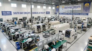
South Bay Circuits (SBC) has operated as a single-source PCB fabrication and assembly partner out of its 60,000 square foot Chandler, Arizona facility since 1981. Its certification scope includes:
- ISO 9001:2015 certification for quality management systems
- AS9100 aerospace compliance
- ISO 13485 compliance for medical device work
- ITAR registration and CMMC Level 1 status
That certification scope matters because potting requirements need to fit into the same accountable process that covers design, fabrication, and assembly. Working with one partner from prototype through production means fewer vendor handoffs and one team responsible for the result, rather than a blame game between separate suppliers.
Frequently Asked Questions
What does potting a circuit board mean?
Potting means encapsulating an assembled board in a liquid compound that cures into a solid or gel-like mass, shielding it from moisture, vibration, and chemical exposure. The mold often remains part of the finished product.
What type of potting compound is used for PCBs?
The three main compound families are epoxy, silicone, and polyurethane. The right choice depends on your application's thermal range, flexibility needs, dielectric requirements, and cure time constraints.
What are PCB potting services?
Potting services refer to a manufacturer's capability to encapsulate assemblies as part of turnkey PCB assembly. This typically includes compound selection guidance, dispensing, and curing as part of the broader production workflow.
Can a potted PCB be reworked or repaired?
Potting is largely permanent once cured, unlike conformal coating, which can be stripped and reapplied. If field rework is a likely need, factor that into your protection method decision before committing to potting.
How long does it take for potting compound to cure?
Cure times vary by compound and temperature: some epoxies cure in a couple of hours at elevated heat, while others need 24 hours or more at room temperature. Always confirm the exact schedule from the compound's technical data sheet.
Does potting affect the weight and size of an electronic assembly?
Yes. Potting adds considerably more weight and bulk than conformal coating because of its greater thickness, which matters for space-constrained or handheld designs.