That dominance creates a real problem for engineering teams. Get an SMT design wrong, and you're looking at solder bridges, tombstoned resistors, or a board that simply won't reflow correctly, each one a potential respin that costs weeks and budget.
This guide walks through what a surface-mount PCB actually is, how it stacks up against through-hole construction, the design decisions that prevent defects, the assembly steps that turn bare boards into working products, and how to pick a manufacturing partner that won't leave you stuck between vendors.
Key Takeaways
- SMT now accounts for the majority of PCBA production, driven by smaller footprints and automated assembly speed
- Component placement, routing, and stencil design decisions made during layout directly determine assembly yield
- Fine-pitch packages like BGA and QFN require via-in-pad techniques and tightly controlled reflow profiles
- Tombstoning, bridging, and voiding trace back to paste volume, heat balance, and pad design, not bad luck
- A single-source manufacturing partner cuts the handoff delays that stack up between design, fabrication, and assembly
What Is a Surface-Mount PCB (SMD)?
What Is a Surface-Mount PCB?
Surface Mount Technology (SMT) attaches components directly to copper pads on the board's surface. No drilled holes, no leads pushed through the board and soldered on the back. The component sits on the pad, solder paste melts during a reflow cycle, and the joint forms in place.
The terminology trips people up, so here's the breakdown:
- SMD (Surface Mount Device): the component itself, like a chip resistor or a QFN package
- SMT (Surface Mount Technology): the manufacturing method used to place and solder SMDs
- SMA (Surface Mount Assembly): the finished assembled board (less common usage)
SMT traces back to the 1960s, with IBM among the early developers of compact surface-attach packaging. It took decades of miniaturization pressure before it became the default choice for nearly everything except high-power connectors and transformers.
Common Package Types
Package size drives how many components fit on a given board area:
| Package Type | Typical Dimensions | Use Case |
|---|---|---|
| 0201 chip resistor/capacitor | 0.60 x 0.30 mm | Ultra-dense passive placement |
| 0402 chip resistor/capacitor | 1.00 x 0.50 mm | Standard passives on most modern boards |
| QFN | ~3.3-3.7 mm square, 0.50 mm pitch | Compact ICs with bottom-terminated pads |
| QFP | 5-28 mm square, 0.40-0.65 mm pitch | Higher pin-count logic devices |
| BGA | Ball pitch as fine as 0.4 mm and below | Processors, memory, high I/O density parts |
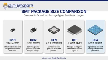
Smaller packages mean tighter pitches, but they also mean less margin for error during stencil design and reflow. That trade-off shows up throughout the rest of this guide.
SMT vs. Through-Hole PCB: Key Differences
Through-hole technology (THT) inserts component leads into plated holes drilled through the board, then solders them on the opposite side. That approach differs from SMT's flat, surface-level attachment in several practical ways.
Density and footprint. SMT allows components on both sides of the board without the drilled-hole clearance THT requires. That frees up routing space and shrinks overall board size, sometimes dramatically.
Assembly method and cost. THT is often hand-solderable, which makes it attractive for one-off prototypes. SMT needs stencils, pick-and-place machines, and reflow ovens, but once that infrastructure exists, it scales far more efficiently for volume production.
Reliability and rework. THT joints handle mechanical stress and vibration well, and a technician can usually rework one with a soldering iron. SMT joints, especially on fine-pitch parts, are more sensitive to thermal cycling and typically need hot-air rework stations or specialized tools.
| Factor | Surface Mount (SMT) | Through-Hole (THT) |
|---|---|---|
| Mounting method | Reflow soldered on surface pads | Leads inserted through plated holes |
| Lead spacing | Fine pitch, down to 0.3-0.4 mm | Wider spacing, hand-solderable |
| Component density | High, both sides usable | Lower, hole clearance required |
| Surface finish needs | Flat, solderable finish critical | Less finish-sensitive |
| Stencil requirement | Yes, for paste deposition | No |
| Rework complexity | Higher, specialized equipment | Lower, manual rework feasible |
Most real-world products don't pick one exclusively. Mixed assembly puts SMT on the logic and signal circuitry while reserving through-hole for parts that need mechanical strength—connectors, large transformers, or power semiconductors with heat sinks.
South Bay Circuits builds this kind of hybrid board regularly, running SMT for density and through-hole for the handful of components that genuinely need it.
Surface Mount PCB Design Process & Best Practices
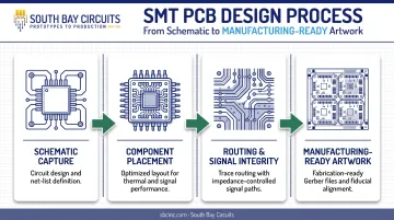
SMT design starts at schematic capture. Pull the correct SMD footprint from your CAD library, verify polarity marks, confirm pin numbers, and double-check reference designators. A wrong footprint at this stage is invisible until the board comes back from assembly with parts that don't fit or sit backward.
Component Placement Strategy
Group components by function, keeping power, signal, and control circuitry in their own zones. High-frequency or noise-sensitive parts belong close together to minimize trace length.
Also plan for the line, not just the schematic:
- Leave clearance for pick-and-place nozzles and reflow airflow
- Avoid packing parts so tight that taller devices shadow neighbors during reflow
Routing and Signal Integrity
Keep traces short and direct to cut resistance and noise pickup. For high-speed signals, control impedance and match differential pair lengths carefully. On dense BGA packages, plan fan-out early using via-in-pad techniques, filled and capped, to avoid trapped gas and voiding underneath the package.
Manufacturing-Ready Artwork
Fiducial marks give pick-and-place machines a fixed reference for alignment. IPC guidance calls for at least two global fiducials, placed diagonally opposite each other. Many panels add a third mark in an "L" pattern for more reliable alignment. Fine-pitch components often need their own local fiducials too.
Finish the artwork with assembly in mind:
- Add tooling holes for panel handling
- Choose V-cut or mouse-bite panelization for small board arrays
- Balance copper coverage across layers and keep the stack-up symmetrical
Warp and twist matter far more for SMT than for through-hole work. An uneven board will not sit flat under a pick-and-place nozzle or track cleanly through a reflow oven.
Surface Mount PCB Assembly Process Step-by-Step
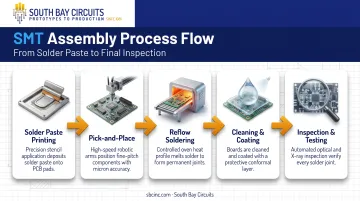
SMT assembly follows a defined, largely automated sequence. Each step depends on the one before it, so a mistake early in the line shows up as a defect much later.
Solder Paste Printing and Stencil Design
A metal stencil, positioned over the board, allows a squeegee to push solder paste through cut apertures onto exposed pads. Stencil thickness and aperture size are matched to the component. Fine-pitch QFN and BGA pads need smaller, precisely sized apertures to prevent bridging or insufficient solder on the joint.
Pick-and-Place and Reflow Soldering
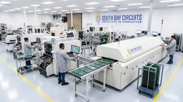
High-speed pick-and-place equipment positions each component using CAD placement data. At South Bay Circuits, Fuji CP-642 and CP-65 chipshooters work alongside a Fuji IP-3 flexible placer with a tray tower, handling everything from tiny passives to tray-fed ICs.
Once populated, the board moves through a reflow oven—BTU VIP 70 or Conceptronic HVA-70 convection systems in production—cycling through preheat, soak, reflow, and cooling. J-STD-020E's classification profile calls for liquidus around 217°C held for 60–150 seconds, with peaks of 245–260°C depending on package thickness. Real production profiles must still respect the specific paste and component limits, not only this classification baseline.
Cleaning, Coating, and Double-Sided Assembly
After reflow, flux residue may need cleaning depending on the paste type and end-use environment. Boards headed for harsh conditions often get conformal coating (silicone, acrylic, or urethane) to guard against moisture and chemical exposure. Double-sided boards get processed in careful sequence so the second reflow pass doesn't re-melt joints already formed on the first side.
Inspection and Testing
Quality checks run throughout, not just at the end:
- AOI (Automated Optical Inspection) scans placement accuracy and joint quality
- X-ray inspection verifies hidden joints under BGA and QFN packages where visual inspection can't reach
- In-circuit and functional testing confirm electrical performance before the board ships
South Bay Circuits uses a Marantz NSPEC FV18 for AOI, a Glenbrook Jewel Box 70T for X-ray inspection, and a Teradyne Z1860VP ICT system with 2,048 test points for electrical verification.
Common SMT Defects and How to Prevent Them
Most SMT defects trace back to paste volume, heat distribution, or pad geometry, not random chance.
| Defect | Root Cause | Prevention |
|---|---|---|
| Tombstoning | Uneven wetting forces lift one end of a small passive | Balance paste deposits and thermal response across the pad |
| Solder bridging | Excess paste or fine spacing causes shorts between pads | Correct stencil aperture sizing, controlled squeegee pressure |
| Insufficient solder | Poor paste transfer or scoop-out during printing | Verify stencil release and paste condition before printing |
| Solder balling | Flux volatilizes too fast or paste oxidizes | Use in-spec paste, control storage, avoid aggressive profiles |
| BGA voiding | Trapped gases escape during reflow, leaving gaps | Optimize stencil design, paste volume, and reflow profile |
Effective prevention combines balanced pad design, correctly sized stencil apertures, a validated reflow profile, and disciplined paste storage that respects shelf life. Consistent yield comes from combining solid Design for Manufacturability (DFM) practices with tightly controlled process parameters on the assembly floor.
A DFM review before committing to production catches most of these issues on paper, where they're cheap to fix, instead of on the assembly line, where they're not. South Bay Circuits builds DFM checks into its standard layout process, flagging manufacturability and testability concerns before a design reaches the line.
Materials, Surface Finishes & Choosing the Right SMT Manufacturing Partner
Surface finish affects both solderability and board flatness. Planar finishes tend to hold up better for fine-pitch SMT than HASL, which can leave uneven coating thickness that interferes with tight-pitch soldering.
| Finish | Strength | Best Fit |
|---|---|---|
| ENIG | Flat, highly solderable, RoHS compliant | Fine-pitch SMT, BGA |
| Immersion Silver | Excellent solderability, slightly lower cost than ENIG | Fine-pitch SMT, general use |
| OSP | Low-cost, planar organic coating | Simpler boards, cost-sensitive runs |
| HASL | Economical, but coating varies across the board | Wider-pitch, less fine-pitch work |
South Bay Circuits offers ENIG and Immersion Silver finishes for its SMT programs.
Laminate choice matters just as much. Lead-free reflow runs hotter and boards see repeated thermal cycling, especially on double-sided or mixed-technology builds, so higher-Tg materials hold up better over the product's life.
South Bay Circuits builds with High-Temperature FR-4 rated at 170°C Tg for these applications, along with Rogers 3000/4000 series and Nelco N4000 series laminates for RF and high-speed designs.
Picking a manufacturing partner matters as much as any design decision. South Bay Circuits runs PCB fabrication and SMT assembly under one roof at its 60,000-square-foot Chandler, Arizona facility. Program credentials include:
- ISO 9001:2015
- AS9100 aerospace compliance
- ISO 13485 medical compliance
- ISO/TS 16949 automotive compliance
That single-source setup removes the file transfers, shipping delays, and vendor handoffs that stack up when design, fabrication, and assembly live at three different companies. Teams often shave days off program launch schedules as a result.
Frequently Asked Questions
What is an SMD, and how does it relate to SMT?
An SMD is a component mounted directly onto PCB surface pads, with no leads through drilled holes. SMT refers to the overall assembly method used to place and solder these components.
What are the key differences between surface-mount and through-hole PCBs?
SMD components sit on surface pads and are joined by reflow soldering; THT parts insert into plated holes. SMT also supports smaller components, higher density, and faster automated assembly than THT.
Can surface-mount and through-hole components be used on the same PCB?
Yes, mixed assembly is common. THT typically handles connectors and power components, while SMT covers logic and signal circuitry on the same board.
What causes tombstoning in SMT assembly?
Tombstoning happens when solder paste volume or heating is uneven between the two ends of a small passive component. One end wets and pulls before the other, lifting the part on its edge.
Which surface finish is best for fine-pitch SMT components?
ENIG and Immersion Silver are preferred over HASL for fine-pitch work, since both provide flatter, more consistent solderable surfaces across dense pad layouts.
Do I need a stencil for a small SMT prototype run?
Stencils are recommended even for prototypes, since they give consistent paste deposition. Very small lots occasionally use manual paste dispensing, but that increases the risk of uneven joints.