Introduction
Automated Optical Inspection, or AOI, is a camera- and software-based quality control process that scans printed circuit boards to detect defects automatically. For PCB manufacturers, design engineers, and quality teams, understanding how AOI actually works matters, especially in aerospace, medical, and automotive programs where a missed defect can mean a safety issue or a failed audit.
AOI gets referenced constantly in electronics manufacturing conversations, yet the operational details often stay vague. How does it actually catch a defect? What makes it miss one? Where does it fall short?
This guide breaks down how AOI works step-by-step, where it fits into production, what affects its accuracy, and when it isn't the right tool for the job.
Key Takeaways
- AOI compares scanned PCB images against a golden standard to flag missing components, misalignment, and soldering defects.
- Three core steps drive the process: image capture, comparison, and defect verification.
- Accuracy depends on lighting, camera resolution, and how well the reference data is maintained.
- Hidden solder joints under BGAs and similar packages need X-ray; AOI cannot inspect them.
- It works best as one layer in a broader quality strategy, not a standalone check.
What Is Automated Optical Inspection?
AOI is an automated visual quality control method. Cameras and image-processing software scan a PCB during or after assembly and flag any deviation from an approved reference. The goal is straightforward: catch visible surface and placement defects before a board moves further down the production line, where fixing the same problem gets more expensive and more disruptive.
AOI is often confused with a few related processes:
- Manual visual inspection — relies on a human eye. Slower, more subjective, and inconsistent across shifts or inspectors.
- X-ray inspection — sees hidden or internal solder joints, such as those under a BGA, that AOI's cameras physically cannot capture.
- Electrical/functional testing — verifies that a board performs correctly, not that it looks correct.
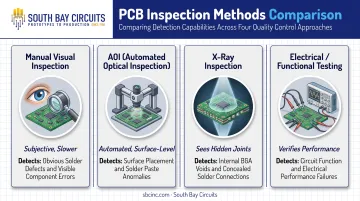
None of these replace each other. They cover different failure modes.
Why AOI Is Used in PCB Manufacturing
Modern boards pack components tighter than ever. A component package known as 01005 measures just 0.2 x 0.4 mm. Manufacturer research has flagged human inspection of parts this small as extremely difficult, if not impractical, at production speed (Vi Technology's 01005 inspection challenges paper).
At that scale, manual inspection simply can't keep pace without sacrificing consistency.
PCB manufacturing in regulated markets demands:
- Repeatable accuracy across every unit on a run, not just the first few
- Traceability — documented proof of what was inspected and when
- Tight tolerances that regulated end markets require by contract
Without AOI, manufacturers typically see inconsistent manual inspection calls, slower defect feedback loops, and higher rework rates downstream. That's why AOI is treated as industry best practice, referenced across IPC workmanship guidelines.
SBC incorporates AOI checks at multiple points in its ISO 9001:2015, AS9100, and ISO 13485 compliant manufacturing flow to support customers building for aerospace, medical, and automotive end uses.
How AOI Works (Conceptual Flow)
AOI follows a repeatable loop: capture an image, compare it to a reference, flag anything that deviates, then route flagged units for human confirmation. Three inputs make this possible:
- A golden board or a CAD/BOM-derived reference profile
- Calibrated lighting set to specific angles
- A camera and lens configuration tuned for the board's component density
The system captures high-resolution images of each inspection zone and runs pixel-level or pattern-matching comparisons against that approved reference. Programmed tolerance thresholds and lighting adjustments keep the algorithm from over-flagging harmless variations, known in the industry as false calls or pseudo-defects.
The result: each board gets a pass/fail determination, a documented inspection report, and any flagged unit gets routed to a technician for review or rework.
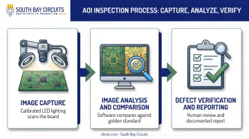
Step 1: Image Capture
Calibrated LED lighting, positioned at multiple angles, illuminates the board while one or more cameras scan it. Depending on the system, this happens in a stop-and-go sequence or a continuous pass, capturing detailed images of each inspection zone as the board moves through.
Step 2: Image Analysis and Comparison
Software compares the captured images against the golden standard or CAD-derived profile. Pattern recognition algorithms scan for deviations such as a shifted component, a missing solder joint, or an unexpected shadow, and flag anything that exceeds the programmed tolerance.
Step 3: Defect Verification and Reporting
A technician reviews every flagged area to confirm whether it's a true defect or a pseudo-defect caused by lighting glare, board color variation, or an overly tight tolerance setting.
SBC's Quality Assurance Assembly Inspectors handle this review using a 10X ring lamp and calipers to verify dimensions against IPC-A-610 and J-STD-001 requirements, recording defect codes and pass/fail results. Once confirmed, the system generates a documented report, and tolerances may get refined for future production runs.
Where AOI Is Applied and What Affects Its Performance
Where AOI Fits Into PCB Manufacturing
AOI shows up in a few common configurations:
- Inline: built directly into the assembly line, inspecting every board as it moves through
- Offline: standalone systems used for detailed inspection without holding up the line
- Statistical sampling setups: used on some high-speed lines where full inspection isn't practical
Two lifecycle points are typical. Boards are checked right after component placement for presence, position, and orientation, then again after soldering or reflow for coplanarity, bridging, and solder integrity. Inspection data often feeds directly back into process control within the broader fabrication and assembly workflow.
AOI can run as a recurring, board-by-board check on standard production runs, or as a condition-based validation step during new product introduction, where inspection criteria get set up and tested before volume production begins.
SBC applies AOI checks at multiple stages of its fabrication and assembly process, including a 100% AOI scan of inner layers during PCB fabrication, as part of its documented quality system.
Key Factors That Affect AOI Accuracy
Several variables determine how well an AOI system actually performs:
| Factor | Why It Matters |
|---|---|
| Board/component density | Smaller, tighter-packed parts need finer resolution to inspect reliably |
| Lighting and calibration | Directly affects contrast and how visible a defect appears |
| Camera resolution and lens quality | Determines the tradeoff between inspection speed and level of detail |
| Production volume/line speed | Dictates full inspection versus statistical sampling |
| Quality-class requirements | Sets the defect thresholds the system must be programmed to enforce |
Camera performance isn't just about pixel count. Systems need fast sensors and high-capacity data interfaces to keep up. One industry camera example transfers 26-megapixel, 8-bit images at up to 150 frames per second over a 50 Gbps interface (JAI's camera selection guide for AOI systems). Raise resolution without the throughput to match, and you slow the whole line down.
IPC Class 2 versus Class 3 requirements also shape how tightly an AOI system gets programmed. Higher classes demand tighter defect thresholds, with less tolerance for visual variation that would pass at a lower class.
Common Issues, Misconceptions, and When AOI Isn't the Right Fit
Common Issues and Misconceptions
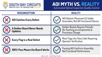
A few assumptions cause real problems on the production floor:
- "AOI catches every defect." It doesn't. Hidden joints under components like BGAs stay invisible to a camera. X-ray inspection covers that gap.
- "The golden board doesn't need updates." It does, especially after a design revision or component substitution. An outdated reference produces bad comparisons no matter how good the camera is.
- "Every flag is a real defect." Many flags are pseudo-defects. One industry example found 15 to 25 pseudo-defects on a 5,000-interconnection SMT board even at 99.5% to 99.7% first-pass yield (Circuits Assembly analysis). Technician judgment stays part of the process.
- "A 100% AOI pass means the board works." It doesn't. AOI confirms visual geometry, not electrical performance. Functional or in-circuit testing still has to verify the board works.
SBC pairs AOI with X-ray equipment for hidden BGA joints and in-circuit testing for electrical parameters, rather than relying on visual inspection alone.
When AOI May Not Be Appropriate
AOI isn't automatically the right call for every job:
- Extremely low-volume prototype runs — setting up and programming inspection criteria for a handful of boards can take longer than a careful manual review.
- Frequent product mix changes — constant reprogramming of inspection recipes eats into the time savings AOI is supposed to deliver.
- Hidden solder joint concerns — X-ray inspection is the better tool when the question is what's happening under a BGA, not on the surface.
- Electrical performance questions — ICT or functional testing answers those; AOI can't.
One warning sign worth watching for: applying unchanged inspection criteria to new, more complex components without recalibrating. That's a signal AOI is being used out of habit rather than by actual need.
Conclusion
AOI is an automated, camera-and-software-driven inspection process. It compares scanned PCB images against a reference standard to catch visible defects consistently and at scale, without the fatigue and variability of manual review.
For manufacturers in regulated industries, knowing how AOI works matters when quality, safety, and compliance are on the line.
AOI works best as one layer in a broader quality strategy. Pair it with X-ray for hidden joints and functional testing for electrical performance instead of relying on it alone.
South Bay Circuits (SBC) builds AOI into its single-source PCB fabrication and assembly process, alongside X-ray and in-circuit testing. That mix helps aerospace, medical, and automotive customers get reliable, compliant results from prototype through volume production.
Frequently Asked Questions
What is an automated optical inspection system?
It's a combination of hardware (cameras and calibrated lighting) and software that scans a PCB and compares the images against a reference standard. Any deviation beyond programmed tolerances gets flagged automatically for review.
What defects can automated optical inspection equipment detect?
Common flags include missing or misaligned components, solder bridging or insufficient solder, wrong polarity, and surface-level scratches or stains. It catches anything visible that deviates from the approved reference.
How much does automated optical inspection equipment cost?
Cost varies widely based on system type (2D versus 3D, inline versus offline) and board size capacity. Most contract manufacturers factor this into per-board inspection pricing rather than customers purchasing equipment directly.
What is the difference between AOI and X-ray inspection?
AOI inspects visible surface features using cameras, while X-ray reveals hidden solder joints under components like BGAs that a camera can't see. The two are complementary, not interchangeable.
Is AOI required to meet PCB quality standards like IPC Class 3?
Not explicitly mandated by IPC documentation, but AOI is widely used as standard practice to consistently meet the tighter tolerance and defect-rate requirements that higher IPC classes demand.
How accurate is automated optical inspection?
Accuracy depends on lighting quality, camera resolution, and how well the gold standard is maintained. Technician verification of flagged items helps manage false calls without letting real defects slip through.