Introduction
Planar transformer PCB design builds flat, etched copper winding patterns directly into multilayer PCB layers. Those windings replace hand-wound wire coils and pair with a low-profile magnetic core.
This guide is for power electronics and PCB design engineers working on industrial, aerospace, medical, automotive, and telecom/server power applications. In those markets, compact, high-reliability power conversion is non-negotiable.
Planar transformers show up constantly in SMPS design literature, yet the layout, stackup, and fabrication decisions behind them get far less attention. Many engineers know the concept but struggle when it's time to specify layer count, interleaving, and core selection.
This article walks through how the design process actually works, what factors drive the outcome, and when planar construction is the right call versus a conventional wire-wound part.
Key Takeaways
- Planar transformers etch primary and secondary windings as flat copper traces, then mate the PCB with a separate ferrite or similar core.
- Lower profile and tighter parasitics come with upfront stackup, interleaving, and thermal design work.
- Design flow: electrical spec → core selection → stackup → winding layout → thermal/EMI checks → fab.
- High-frequency SMPS designs in space-constrained, high-reliability builds gain the most.
- Low-frequency or highly variable windings still favor conventional wire-wound transformers.
What Is Planar Transformer PCB Design?
Planar transformer PCB design means engineering flat copper conductor patterns across PCB layers so they function as the primary and secondary windings of a transformer. Once fabricated, that PCB gets mated with a ferrite or similar magnetic core to complete the part.
The goal is the same voltage transformation and isolation as a conventional transformer—in a flat, repeatable, PCB-manufacturable form. That layout gives the designer tighter control over leakage inductance and parasitic capacitance than a hand-wound bobbin ever could.
Engineers sometimes confuse it with two related but different disciplines:
- Standard multilayer PCB design – not built to carry inductive windings or manage the current density and thermal loads a transformer winding sees.
- Conventional wire-wound transformer manufacturing – manual coil winding on a bobbin around a core, with all the variability that implies.
Two Ways to Implement It
Engineers generally pick one of two approaches:
- Standalone planar transformer component – its own small PCB plus core, mounted onto the main board like any other discrete part.
- Fully integrated windings – the transformer windings live directly inside the main PCB layout, sharing layers with other circuitry.
In both cases, fabrication of the PCB itself typically happens without the magnetic core in place. The core gets added afterward, so you can choose the geometry that fits the application—E-core, U-core, or toroidal.
Why Planar Transformer PCB Design Matters
Modern SMPS and isolated DC-DC converter designs demand three things simultaneously: compactness, thermal performance, and manufacturing repeatability. Flat PCB windings address all three better than hand-wound coils, which vary from unit to unit no matter how skilled the winder.
Skip planar construction where it's warranted, and the problems show up fast:
- Bulky, tall transformers that blow past height budgets in dense boards.
- Inconsistent leakage inductance between units built by different winders or on different days.
- Thermal bottlenecks from wire bundles that don't dissipate heat as efficiently as flat copper.
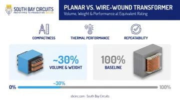
One frequently cited industry comparison puts a planar transformer at roughly 30% of the volume and weight of a traditional wire-wound transformer of equivalent rating. That's not a universal number for every design, but it's a useful sense-check when you're weighing the switch.
Planar magnetics show up most often in these topologies:
| Topology | Common Application |
|---|---|
| Flyback | Industrial power supplies, medical devices |
| LLC resonant | Telecom/server power, EV chargers |
| Forward converter | Aerospace power modules |
| Phase-shifted full bridge | High-power industrial, EV charging |
Performance still drives adoption—density, efficiency, and unit-to-unit repeatability—not regulation alone. Aerospace, medical, and automotive programs add compliance on top, and those rules shape PCB stackup, copper weight, and fab choices later in the design.
How Planar Transformer PCB Design Works (Design Flow)
The process starts from an electrical specification and works backward. Voltage, power, frequency, and topology feed into calculations that determine core size, turns count, and PCB layer stackup, all constrained by flux density and thermal limits.
The output is a manufacturable PCB layout with integrated windings. Once mated with a magnetic core, that board functions as a transformer meeting the target inductance, isolation, and thermal specification.
Step 1: Define Specifications and Select the Core
Gather your input/output voltage, power, switching frequency, and topology first. From there, apply Faraday's Law and the area-product method to size the core and calculate primary turns.
For a square-wave design, the area-product relationship looks like this:
Ae × Aw = Smax / (Kf × Kr × Bpeak × Jmax × fs)
Where:
- Ae — magnetic cross-section
- Aw — window area
- Smax — apparent power
- Kf — waveform factor
- Kr — window fill factor
- Bpeak — peak flux density
- Jmax — current density
- fs — switching frequency
Faraday's equation for the same design gives Bpeak = Vi / (4 × Nc × Ae × fs), using a form factor of 4 for a square wave rather than 4.44 for a sinusoid as detailed in a peer-reviewed planar transformer sizing study.
Choose core material grade and geometry based on frequency and a peak flux density that leaves thermal headroom below saturation. An equivalent planar core often runs one size smaller than its wire-wound counterpart—verify that with your own area-product calculation rather than assuming it.
Step 2: Plan Layer Stackup and Winding Layout
Calculate secondary turns from the turns ratio, then distribute those turns across PCB layers. Interleave primary and secondary windings, commonly in a P-S-P or S-P-S arrangement, to control leakage inductance and AC winding losses.
Set the remaining layout parameters against the safety standard for your end product:
- Trace width and copper weight for current density
- Via interconnects between winding layers
- Creepage and clearance distances for isolation
Commercial planar designs are often limited to about a 6:1 turns ratio. Higher ratios drive layer count and complexity past the point where a flat winding still makes sense.
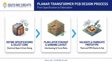
Step 3: Validate and Fabricate the Prototype
Run thermal simulation that accounts for AC winding losses from skin and proximity effect, not just DC resistance. Follow with EMI checks before fabrication. On the built prototype, verify:
- Magnetizing inductance
- Leakage inductance
- Isolation voltage against design targets
Planar transformer PCBs demand precise multilayer registration and tightly controlled dielectric thickness between winding layers. Fast revision turnaround matters, because the stackup is rarely right on the first pass.
Partnering with a single-source fabricator and assembler, such as South Bay Circuits, keeps design, fabrication, and assembly under one roof. Process knowledge and test data stay with the design instead of getting rebuilt at every vendor handoff.
Key Factors That Affect the Design
Several variables determine whether your planar transformer performs the way your simulation predicted:
- Core material and geometry – ferrite grade, E-core, U-core, or toroidal shape affects flux density, core loss, and thermal behavior.
- Copper weight, trace width, and layer count – these set current-carrying capacity and DC resistance for each winding.
- Interleaving pattern and dielectric thickness – controls leakage inductance, inter-winding capacitance, and isolation voltage.
- Switching frequency and topology – dictates achievable turns count, realistic core size, and whether planar is viable at all.
- Safety and regulatory requirements – creepage/clearance under IEC 62368-1 and sector rules (automotive, medical) scale with working voltage, material group, and pollution degree—not a single fixed spacing.
Manufacturing Tolerances Matter Just as Much as the Schematic
A stackup only performs as designed if the fabricator holds registration and dielectric tolerances consistently. Multilayer registration, controlled dielectric thickness, and heavy-copper processing decide how closely the finished board matches simulated inductance and loss.
South Bay Circuits, for example, supports 2 oz copper winding layers with trace width and spacing down to 0.010"/0.010" under standard technology, or 0.007"/0.007" where tighter process capability is required, plus blind and buried vias to interconnect winding layers.
Every panel runs with test coupons, full AOI on inner layers, and X-ray plus micro-section checks for registration and dielectric consistency.
Choosing a fabricator certified for your market—ISO 13485 (medical), AS9100 (aerospace), or IATF 16949 (automotive)—also cuts requalification risk as you move from prototype to volume.
Common Issues, Misconceptions, and When Planar May Not Be Appropriate
A few misconceptions trip up even experienced engineers moving to planar for the first time.
"Planar transformers are always smaller overall." Height drops significantly, sometimes dramatically. But PCB width and depth footprint often increase to fit the same winding area flat. Total board area isn't automatically reduced, just reshaped.
"More turns means more layers." Actual layer count depends on interleaving pattern, current capacity per layer, and isolation requirements, not turns count in isolation. Two designs with identical turns can need very different layer counts.
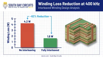
"DC resistance tells the whole story." It doesn't. Skin and proximity effect can dominate total loss at high switching frequencies if the stackup isn't optimized. One manufacturer's worked example shows winding losses dropping from 4.2 W with no interleaving to 1.6 W fully interleaved at the same 400 kHz operating point, purely from stackup changes.
When planar stops making sense:
- Low switching frequencies outside the typical high-frequency SMPS range, where core losses and turns count work against a flat design
- Low-volume prototypes or highly variable windings, where PCB tooling lead time beats a quick hand-wound iteration
- Default selection without validation—if turns ratio, current, and footprint haven't been checked against real PCB winding limits, "modern" and "compact" aren't reasons enough
Frequently Asked Questions
What is a planar transformer?
A planar transformer replaces wire-wound coils with flat copper traces etched into PCB layers, paired with a low-profile magnetic core. It still relies on the same electromagnetic induction principle as a conventional transformer to step voltage up or down.
What are the advantages of using a planar transformer?
Planar transformers offer higher power density, a lower profile, and better thermal dissipation than wire-wound units. They also deliver more consistent, repeatable manufacturing since flat copper traces don't vary unit to unit the way hand-wound coils do.
How is a planar transformer different from a conventional wire-wound transformer?
Planar designs use flat PCB copper windings instead of manually wound wire coils. That translates to lower height, lighter weight, tighter leakage inductance control, and better production repeatability.
What frequency range do planar transformers typically operate at?
Most planar transformers operate in high-frequency switch-mode power supply (SMPS) designs, typically 20 kHz to 2.5 MHz. Higher switching frequency reduces the turns count and layer count needed, which shrinks overall size.
Can a planar transformer be fully integrated into a PCB assembly, or does it need a separate core?
Windings can be integrated into the main PCB layout or built as a standalone component. Either way, the magnetic core is almost always added after PCB fabrication rather than built in.
Is a planar transformer PCB more expensive to manufacture than a conventional transformer?
At low volumes, yes, largely due to PCB tooling costs. At scale, planar designs often become more cost-effective once fabrication consistency, thermal performance, and assembly savings are factored in.