PCB X-ray inspection, often called AXI (Automated X-ray Inspection), is the non-destructive method manufacturers use to see through the board and catch these hidden defects before a product ships. Instead of relying on what's visible on the surface, X-ray imaging penetrates the substrate and solder to reveal what's happening underneath.
This guide walks through the equipment you need, the inspection methods available, how to read the resulting images, the mistakes that trip up even experienced operators, and the safety protocols that keep the process defensible.
Key Takeaways
- AXI catches what AOI and ICT miss: voids, bridges, and BGA/QFN misalignment under components
- 2D X-ray suits fast, high-volume screening; 3D/CT separates overlapping layers on dense boards
- Judge results against IPC-A-610 acceptance criteria, not gut feel
- Accuracy depends on calibration, trained operators, and radiation safety controls
What You Need for PCB X-Ray Inspection
Good results start before the X-ray tube ever powers on. The right equipment, a clean board, and correctly tuned settings determine whether an image actually reveals a defect or just introduces noise that leads to a bad call.
Equipment and Tools Required
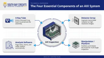
A functional AXI setup requires four core components:
- X-ray tube (open or sealed) — generates radiation that penetrates the board. Open tubes offer higher resolution but need regular maintenance; sealed tubes skip routine servicing but have a fixed service life.
- Detector array — converts transmitted photons into a viewable grayscale image
- Manipulator/platform — tilts and rotates the board so operators can view solder joints from multiple angles, not just straight down
- Analysis software — measures void percentage and flags defects against IPC-A-610 criteria automatically, rather than leaving every call to visual judgment
Preconditions and Setup
A few setup steps make the difference between a repeatable inspection and a guessing game:
- Mount the board securely on a clean, contaminant-free surface — any movement during the scan blurs the image and can hide real defects
- Tune voltage and magnification to the board's thickness and component density
- Engage shielding and safety interlocks before powering on the source
- Run a known-good reference board through the system first to confirm calibration before inspecting production units
As a reference point, Viscom's iX7059 runs a sealed 130 kV tube with a 160 kV option for dense assemblies — exact settings still vary by system and board.
Skip any of these steps and you risk chasing phantom defects — or missing real ones.
Methods to Perform PCB X-Ray Inspection
Which method makes sense depends on three things:
- How complex the board is
- What type of defect you're hunting
- How fast you need to move units through the line
Method 1: 2D X-Ray Inspection
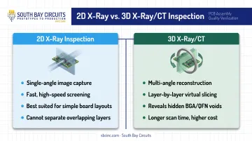
Description: Captures a single-angle transmission image. Works well for simpler boards and high-speed screening where depth separation isn't critical.
Tools needed: X-ray tube, flat panel detector, manipulator with basic tilt function.
Steps:
- Position and secure the PCB on the inspection platform
- Set voltage and magnification for the target component (BGA, QFN, etc.)
- Capture and review the grayscale image for shadow contrast indicating voids or bridges
Trade-off: Fast and cost-effective, but overlapping components on multilayer boards can mask defects that a single-angle image simply can't separate.
Method 2: 3D X-Ray / Computed Tomography and Laminography
Description: Builds a 3D reconstruction from multiple angled 2D images. This is the method for dense, multilayer assemblies where defects hide behind other structures.
Tools needed: Rotating stage or multi-angle source/detector setup, CT reconstruction software.
Steps:
- Rotate the board (or the source/detector array) through defined angular increments
- Reconstruct cross-sectional slices using the CT algorithm
- Review the model layer by layer for voids, cracks, and misalignments
Trade-off: Reconstructed slices separate overlapping structures that stay superimposed in a 2D projection, which is exactly why 3D catches head-in-pillow and hidden QFN voiding that 2D can't. The cost is longer scan times and pricier equipment.
Method 3: Automated (Online) vs. Manual (Offline) Inspection
Description: Online systems run programmed scans directly on the production line. Offline systems inspect sampled units afterward, usually for failure analysis or spot checks.
Tools needed: Programmable Automated X-ray Inspection (AXI) software with pass/fail thresholds (online), or an operator-guided review station (offline).
Steps:
- Define inspection parameters and acceptance thresholds in the software
- Run the scan on every unit (online) or select sample units for manual review (offline)
- Flag any unit outside tolerance for engineering follow-up
Trade-off: Online suits high-volume, consistent screening. Offline is more economical for low-volume runs or one-off failure investigations.
How to Interpret PCB X-Ray Inspection Results
Misreading an image cuts both ways — a defective board ships, or a perfectly good one gets scrapped for nothing. Neither outcome is cheap, which is why interpretation matters as much as the scan itself.
IPC-A-610 is the standard reference for acceptance criteria. The current revision, IPC-A-610J, was released in April 2024 and remains the benchmark manufacturers use to judge voiding, opens, and shorts.
Exact numeric thresholds vary by product class (Class 1, 2, or 3), so always check the licensed standard against your contractual requirements rather than relying on a generic percentage.
| Finding | What it looks like | Action |
|---|---|---|
| Normal/Acceptable | Uniform, dark solder fillets, minimal voiding within IPC-A-610 tolerance, fully seated BGA balls | Approve for next production step |
| Minor Issues | Small, isolated voids or slight misalignment still within IPC-A-610 limits | Log for trend monitoring; no rework triggered |
| Out-of-Spec | Large voids, solder bridges/shorts, open circuits, missing or misaligned components | Flag for rework, rejection, or failure analysis |
Consistency matters here. The same board scanned by two operators, at two different magnification settings, should still land in the same category.
Common Errors in PCB X-Ray Inspection
Even well-run inspection programs run into the same handful of mistakes:
- Misreading shadow artifacts as solder defects: overlapping components at a poor viewing angle can look exactly like a void or bridge that isn't actually there
- Relying only on 2D imaging for multilayer boards, where hidden defects sit behind other structures and need 3D/CT depth analysis to confirm
- Skipping routine calibration, which lets void-percentage readings drift over weeks or months without anyone noticing until a customer complaint arrives
- Using inconsistent board placement or magnification settings between operators or shifts, producing results that don't repeat and making trend data useless
Most of these trace back to the same root cause: treating the X-ray step as a quick pass/fail checkbox instead of a calibrated measurement process.
Safety and Best Practices
X-ray inspection is safe when the protocols around it are followed — but the protocols exist for a reason.
- Maintain shielding, interlocks, and dosimetry. FDA compliance guidance for cabinet X-ray systems caps emission at 0.5 mR per hour at 5 cm outside the cabinet and requires redundant door interlocks. Operator dosimetry monitoring should be part of the routine, not an afterthought.
- Schedule regular calibration and maintenance so imaging and void-percentage reporting stay accurate over time, not just on installation day.
- Use trained, certified operators familiar with IPC-A-610 and J-STD-001 criteria. A defensible inspection call depends on the person reading the image, not just the machine capturing it.
- Layer X-ray with AOI and ICT. Each catches something the others miss — AOI verifies surface placement, ICT checks electrical continuity, and X-ray exposes what's hidden underneath.
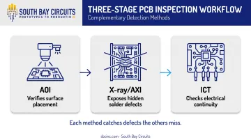
That layered model works best when it stays in-house. South Bay Circuits runs AOI, X-ray inspection, and ICT inside its Chandler, Arizona assembly process rather than sending boards out. Keeping assembly and inspection under one roof folds X-ray into the existing workflow and avoids the queue and shipping delays of a separate inspection vendor.
Consistent, well-calibrated X-ray inspection catches hidden defects before they become field failures. It also gives a clear, defensible call on whether a board ships or goes back for rework.
Frequently Asked Questions
What is PCB X-ray inspection?
PCB X-ray inspection, or Automated X-ray Inspection (AXI), is a non-destructive test that uses X-ray radiation to reveal internal defects like solder voids, bridges, and component misalignment. These issues are invisible to standard optical inspection.
How much does a PCB X-ray inspection machine cost?
Pricing varies widely by configuration: 2D systems cost less than inline 3D/CT platforms, and tube design affects both upfront and maintenance costs. Many manufacturers skip the equipment purchase entirely and outsource inspection to a contract manufacturer with in-house AXI capability.
What defects can X-ray inspection detect that AOI cannot?
X-ray exposes hidden BGA and QFN solder joints, internal voids, head-in-pillow defects, and multilayer trace issues buried beneath the surface. AOI only sees what a camera can: the optically accessible top and bottom of the board.
What is the difference between 2D and 3D X-ray inspection?
2D captures a single-angle image, which is fast but can't separate overlapping structures on dense boards. 3D/CT reconstructs layer-by-layer slices, giving depth accuracy that's essential for multilayer or high-density designs.
Is PCB X-ray inspection safe for operators?
Yes, when systems are properly shielded and interlocked. Cabinet X-ray systems are designed to contain radiation well below regulatory limits, and dosimetry monitoring adds another layer of protection for operators.
When should I use X-ray inspection instead of relying only on AOI or ICT?
Use X-ray for boards with hidden solder joints like BGAs or QFNs, dense multilayer designs, or when you need root-cause failure analysis. AOI and ICT are faster but can't see what's hidden.